You are currently viewing SemiWiki as a guest which gives you limited access to the site. To view blog comments and experience other SemiWiki features you must be a registered member. Registration is fast, simple, and absolutely free so please,
join our community today!
Mining assertions from constrained random simulations to localize bugs. Paul Cunningham (GM, Verification at Cadence), Jim Hogan and I continue our series on research ideas. Feel free to comment.
The Innovation
This month’s pick is Symptomatic bug localization for functional debug of hardware designs. This paper was presented… Read More
Alphawave IP is a new member of the SemiWiki community. You can learn about the company and their CEO, Tony Pialis in this interview by Dan Nenni. Design & Reuse did a virtual IP-SOC Conference recently and Tony presented. The D&R event had a very strong lineup of presenters. They supplemented the prepared video presentations… Read More
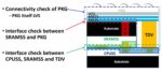
Design Considerations for 3DICsby Tom Dillinger on 12-14-2020 at 6:00 amCategories: Events, Foundries, TSMC
The introduction of heterogeneous 3DIC packaging technology offers the opportunity for significant increases in circuit density and performance, with corresponding reductions in package footprint. Yet, the implementation of a complex 3DIC product requires a considerable investment in methodology development for all… Read More
I used to be part of the custom silicon management team at Apple. I’ve seen how great a challenge it is to pull off a custom silicon strategy within a one year product cycle. Apple is the perfect example of this custom silicon model since they develop the best mobile processors in the world for their products. Which also includes other… Read More
What is the “right track” for US-China trade relations?
The semiconductor industry has been squarely in the crosshairs of US-China trade tensions for four years. As the US faces a presidential leadership transition, will a Biden administration change the dynamic? The chip industry is counting on it, and China hopes so too.
In … Read More
David Zipper of Harvard’s Kennedy School writes in Slate that the incoming Biden Administration should “bring the hammer down” on Tesla Motors for its mis-labeled and therefore misleading Autopilot application and the recently updated Full Self-Driving software beta in the interest of the general public. Zipper’s plan,
…
Read More
Everyday, engineers are running simulations to deliver the next generation of products to make our lives better. Everyday, they wait for those simulations to finish, wishing that they could get answers instantaneously. While waiting for those simulations or checking on the status of their runs at night, they might indulge in… Read More
All semiconductor design work today rests on the three-legged stool of Foundries, EDA Tools and Designers. Close collaboration between the three make possible the successful completion of ever more complex designs, especially those at advanced nodes. Perhaps one of the most critical intersections of all three is during physical… Read More
As I have discussed before, I believe that IEDM is the premier technical conference for understanding leading edge process technologies. Beginning this coming weekend, this year’s edition of IEDM will be held virtually, and I highly recommend attending.
The conference held a press briefing last Monday. The tutorial and short… Read More
Altair is a broad-based technology company with an ambitious vision. As stated on their website: Our comprehensive, open-architecture solutions for data analytics, computer-aided engineering, and high-performance computing (HPC), enable design and optimization for high performance, innovative, and sustainable products… Read More


Musk’s Orbital Compute Vision: TERAFAB and the End of the Terrestrial Data Center