You are currently viewing SemiWiki as a guest which gives you limited access to the site. To view blog comments and experience other SemiWiki features you must be a registered member. Registration is fast, simple, and absolutely free so please,
join our community today!
One of the more interesting parts of blogging for SemiWiki is getting to know emerging EDA and IP companies from around the world. As I have mentioned before, there are some incredibly intelligent people in the fabless semiconductor ecosystem solving very complex problems. It is a two way exchange of course since we know the market… Read More
In the old days to learn about new semiconductor IP you would have to schedule a sales call, listen to the pitch, then decide if the IP was promising or not. Today we have webinars which offer a lot less drama than a sales call, plus you get to ask your questions by typing away at the comfort of your desk, hopefully wearing headphones as … Read More
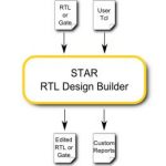
DeFacto and their STAR technology are already quite well known among those who want to procedurally apply edits to system-level RTL. I’m not talking here about the kind of edits you would make with your standard edit tools. Rather these are the more convoluted sort of changes you might attempt with Perl (or perhaps Python these days).… Read More
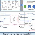
Clock Domain Crossing (CDC) is a common occurrence in a multiple clock design. In the FPGA space, the number of interacting asynchronous clock domains has increased dramatically. It is normal to have not hundreds, but over a thousand clock domains interactions. Let’s assess why CDC is a lingering issue, what its impact and the … Read More
Today more than ever where you live may well determine what kind of car you drive. Federal governments and, lately, cities are stepping forward to determine what kinds of cars are available to consumers and how they will be built.
The latest such initiatives are efforts by the Trump Administration in the U.S. to explore lowering … Read More
With each new silicon process node, the complexity of SoC design rules and physical verification requirements increases significantly. The foundry and an EDA vendor collaborate to provide a “reference flow” – a set of EDA tools and process design kit (PDK) data that have been qualified for the new node. SoC design methodology … Read More
In the EDA space, nothing seems to be more fragmented in-term of solutions than in the Design Verification (DV) ecosystem. This was my apparent impression from attending the four panel sessions plus numerous paper presentations given during DVCon 2018 held in San Jose. Both key management and technical leads from DV users community… Read More
The time is 1995 and my mandate as Layout Manager is to grow my team. I advertised everywhere but there were no experienced people in Canada that I can hire so the solution was back to training. I was the trainer a few times in Israel in MSIL but there we had a very organised material for layout, UNIX, software, etc. We had exercises, tests,… Read More
Thanks to my growing involvement in formal (at least in writing about it), I was happy to accept an invite to this year’s Oski DVCon dinner / Formal Leadership Summit. In addition to Oski folks and Brian Bailey (an esteemed colleague at another blog site, to steal a Frank Schirrmeister line), a lively group of formal users attended… Read More
The semiconductor industry has gone through several major transitions driven by different dynamics such as shift in business models (fab-centric to fab-less), product segmentation (system design house, IP developers) and end market applications (PC to cloud; and recently, to both automotive and Internet of Things — IOT’s,… Read More


Should the US Government Invest in Intel?