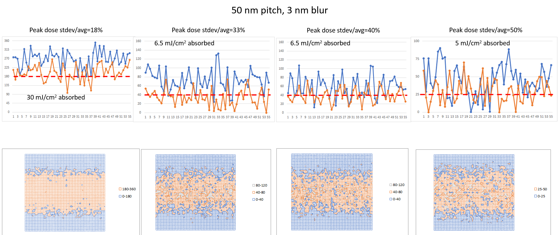
The majority of EUV production is on 5nm and 3nm node, implemented by late 2022. Metal oxide resists have not been brought into volume production yet [1,2], meaning that only organic chemically amplified resists (CARs) have been used instead until now. These resists have a typical absorption coefficient of 5/um [3,4], which means 33% absorption in 80 nm thick resist. This absorption is not that much really, and smaller features require thinner resists in order to maintain a practical aspect ratio of ~2 [5,6]. This, in turn, exacerbates the stochastic effects from the reduced density of photon absorption and subsequent secondary electron generation (Figure 1).

Figure 1. Secondary electrons per nm2 for 50 nm pitch, 3 nm blur, at different absorbed doses and different ratios of peak dose standard deviation to average. Blue: peak dose; orange: edge dose. Red line indicates the printing threshold.
The lower dose leads to a larger variation of secondary electron density, as indicated by standard deviation/average at the peak dose contour (center of bright line) or edge dose contour (half-pitch edge). This is consistent with larger line edge roughness as well as general dose uniformity. The larger variation ultimately comes from standard deviation being equal to the square root of the average; the standard deviation-to-average ratio is inversely proportional to this, which is why it gets higher with lower dose (absorbed photon density).
Smaller pitches at the same dose will also suffer worse stochastic variation. The reason for this is the smaller pitch takes up a smaller area, leading to fewer photons per pitch at a given dose. The standard deviation/average ratio is a fluctuating value even for a fixed dose and pitch. The median for the peak dose contour is plotted in Figure 2, showing similar trends vs. dose for different pitches.

Figure 2. Median standard deviation/average ratio for peak dose contour, as a function of pitch (35-60 nm) and incident dose. The CAR resist thickness is taken to be equal to the pitch; the absorbed dose is determined accordingly. A standard deviation-to-average ratio of 30% is taken to be the acceptance criterion
A standard deviation-to-average ratio of 30% is taken to be the acceptance criterion for the median peak dose variation. For this median value, ratios above 30% are still possible and from Figure 1, these values lead to visibly significant dose non-uniformity extending over 1 nm. Clearly, smaller pitches require significantly higher doses. To keep the productivity dose of 30 mJ/cm2 [7], the pitch is restricted to be 60 nm or larger. However, higher doses will hurt the productivity as the throughput will take a hit (Figure 3) [8].

Figure 3. Throughput vs. dose for a hypothetical 375 W source [8].
For example, a dose of 80 mJ/cm2 with a 375 W source leads to a throughput of 80 WPH, which is not cost-effective compared to DUV multipatterning [9]; ~40 mJ/cm2 is currently targeted to maintain acceptable throughput [10]. Moreover, when doses get too high, the nature of the resist is changed, due to crosslinking [11] or outgassing [12]. Uncleared resist results from dose going too far above the threshold level [11,13]. EUV multipatterning with a wider pitch would be the only way to maintain acceptable doses; this has also been indicated by vendors [14,15].
For the metal oxide resists currently under development [1,2,10,16], the absorption coefficient is increased from 5/um to 20/um [4], giving the trends shown in Figure 4. With the higher absorption, a 35 nm pitch may be achieved with 30-40 mJ/cm2. Larger pitches can use even lower doses, which is better for EUV productivity. However, the sub-25 nm pitches for beyond 3nm node will still require multipatterning [15]. An even higher absorption coefficient would be necessary for the thinner resists that are considered for High-NA EUV lithography [8].

Figure 4. Median standard deviation/average ratio for peak dose contour, as a function of pitch (25-60 nm) and incident dose. The metal oxide resist thickness is taken to be equal to the pitch; the absorbed dose is determined accordingly. A standard deviation-to-average ratio of 30% is taken to be the acceptance criterion.
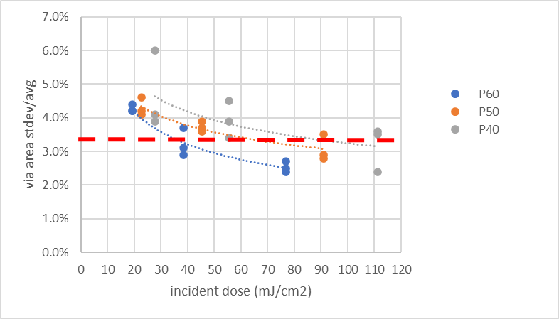
The above cases only apply to line-space patterns. Contacts and vias are evaluated differently [17] as they are circular shapes. Here, the standard deviation-to-average ratio for the enclosed exposed area is used (Figure 5).

Figure 5. Standard deviation/average ratio for via area as a function of incident dose and pitch. The CAR resist thickness is taken to be equal to the pitch; the absorbed dose is determined accordingly. A Gaussian was fitted to the via half-pitch [17]. The fit lines are for guiding the eye only.
To keep the area 3s/avg below 10%, the dose needs to exceed ~35 mJ/cm2 for the 30 nm via but increases quickly as the via shrinks, with the CAR thickness equal to double the via diameter.
The non-EUV doses in an EUV lithography system [18] have not yet been included in the above estimates, because they have been hard to quantify. Presumably they may help to reduce the standard deviation-to-average ratio, allowing lower dose and therefore higher throughput. However, this comes at the price of reduced image contrast, which will in turn degrade the resolution.
References
[1] https://monoist.itmedia.co.jp/mn/articles/2109/21/news038.html
[2] https://english.etnews.com/20221220200003
[3] W. D. Hinsberg et al., J. Micro/Nanopattern. Mater. Metrol. 014603 (2021).
[4] http://euvlsymposium.lbl.gov/pdf/2015/Posters/P-RE-06_Fallica.pdf
[6] https://www.jstage.jst.go.jp/article/photopolymer/16/3/16_3_369/_pdf
[7] https://www.asml.com/en/products/euv-lithography-systems/twinscan-nxe-3600d
[8] H. J. Levinson, Jpn. J. Appl. Phys. 61 SD0803 (2022).
[9] https://semiengineering.com/euv-reaches-a-crossroads/
[10] I. Seshadri et al., IEDM 2023.
[11] I. Pollentier et al., Proc. SPIE 10957, 109570I (2019).
[12] I. Bespalov et al., ACS Appl. Mat. Interfaces, 12, 9881 (2020).
[13] https://www.euvlitho.com/2016/P79.pdf
[15] A. Raley et al., Proc. SPIE 12056, 120560A (2022).
[16] T. Kohyama et al., Proc. SPIE 12498, 124980A (2023); https://www.semiconkorea.org/ko/node/6866
[17] https://www.youtube.com/watch?v=gkiJBwOE6vM
[18] F. Chen, “Non-EUV Exposures in EUV Lithography Systems Provide the Floor for Stochastic Defects in EUV Lithography,” https://www.linkedin.com/pulse/non-euv-exposures-euv-lithography-systems-provide-floor-chen-jymgc
This article first appeared in LinkedIn Pulse: Pinning Down an EUV Resist’s Resolution vs. Throughput
Also Read:
Application-Specific Lithography: Sense Amplifier and Sub-Wordline Driver Metal Patterning in DRAM
Application-Specific Lithography: Avoiding Stochastic Defects and Image Imbalance in 6-Track Cells
Share this post via:


Captain America: Can Elon Musk Save America’s Chip Manufacturing Industry?