The resolution of EUV lithography is commonly expected to benefit from the shorter wavelengths (13.2-13.8 nm) but in actuality the printing process needs to include Pde the consideration of the lower energy electrons released by the absorption of EUV photons. The EUV photon energy itself has a nominal energy range of 90-94 eV, corresponding to 13.2-13.8 nm. Upon absorption, photoelectrons of ~80 eV are released through ionization. These very quickly scatter and lose energy, releasing more electrons (“secondary electrons”) in the process. The energy finally absorbed in the resist film is essentially deposited by these secondary electrons, even with energies as low as around 1 eV [1]. Therefore, the actual resolution of the EUV-printed image is ultimately determined by the spread of these secondary electrons.
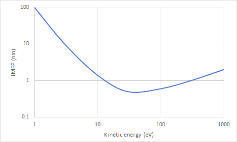
The inelastic mean free path (IMFP) is a parameter commonly used to describe the distance traveled by electrons before scattering with energy loss, i.e., inelastic scattering. It is expected to be on the order of nanometers. Since scattering is itself a random or stochastic event, the IMFP itself would have a range of values. This leads to a range of possible values for the blur in the resist image. The IMFP will depend on the kinetic energy of the electron, characteristically taking a minimum value below around 100 eV [2, 3] (Figure 1).

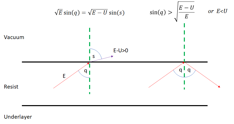
As the energy decreases, the electron is continually traveling through scattering, and potentially may encounter the interface of the resist with the vacuum above it. This top surface has an energy barrier that tends to prevent electrons from escaping. The barrier is equal to the sum of the Fermi energy and the work function, and is also the same as the ionization potential [4]. For one popular tin-based EUV resist material component, SnOH, the ionization potential is 6.6 eV [5]. That means electrons with energies less than this value will be prevented from escaping into the vacuum. They will be reflected back from the top surface. The physics behind this is the conservation of momentum parallel to the interface. The perpendicular component of the momentum is reduced due to the interface barrier [6]. The electron energy in the vacuum upon crossing the barrier is decreased from E to E-U, where U is the barrier energy. The corresponding total momentum magnitude goes from sqrt(2mE) to sqrt(2m(E-U)), where m is the electron mass. The component parallel to the interface is given by sqrt(2mE)sin(q) in the resist, and sqrt(2m(E-U))sin(s), in the vacuum above the resist (Figure 2). These are equal, leading to an equation similar to Snell’s Law of refraction. If E<U, or sin(q)>sqrt([E-U]/E), the presence of the electron in the vacuum is forbidden, and so the electron keeps its initial energy and momentum magnitude E by being reflected at the same energy and angle. This is analogous to the total internal reflection of light at waveguide walls. This tends to give the lowest energy electrons extra opportunity to scatter and spread laterally within the resist, thereby increasing the image blur.

The bottom interface with the resist underlayer would similarly play a key role, as an energy barrier there would increase blur even further with an additional boundary for internal reflection. On the other hand, it may also be a negative energy barrier, allowing electrons to escape the resist film into the underlayer. Hence, we expect the resist underlayer to significantly affect the low-energy electron spread in EUV resists. There is the uncomfortable realization that the EUV-deposited dose, rather than being a certain number of photons absorbed in a square nanometer, is actually an indeterminate number of electrons of unknown trajectories finally resting in that square nanometer.
References
[1] I. Bespalov et al., ACS Appl. Mater. Interfaces 12, 8, 9881 (2020).
[2] M. P. Seah and W. A. Dench, Surf. and Interf. Anal. 1, 2 (1979).
[3] D-N. Le and H. T. Nguyen-Truong, J. Phys. Chem. C 125, 34, 18946 (2021).
[4] A. Klein et al., Materials 3, 4892 (2010).
[5] Y. Zhang et al., Appl. Phys. Lett. 118, 171903 (2021).
[6] O. Yu et al., J. Elec. Spec. and Rel. Phenom. 241, 146824 (2020).
This article first appeared in LinkedIn Pulse: Electron Blur Impact in EUV Resist Films from Interface Reflection
Also Read:
Application-Specific Lithography: 5nm Node Gate Patterning
Spot Pairs for Measurement of Secondary Electron Blur in EUV and E-beam Resists
Share this post via:


Captain America: Can Elon Musk Save America’s Chip Manufacturing Industry?