Lithography has been the driving force for shrinking feature sizes for decades, and the most easily identified factor behind this trend is the reduction of wavelength. G-line (436 nm wavelength) was used for 0.5 um in the late 1980s [1], and I-line (365 nm wavelength) was used down to 0.3 um in the 1990s [2]. Then began the era of deep-ultraviolet (DUV), during which two wavelengths, KrF (248 nm) and ArF (193 nm) dominate even today. Subsequent wavelengths were practically impossible to find. Both F2 (157 nm) and EUV (13.2-13.8 nm) suffer from strong absorption in air. 157 nm required a dry nitrogen ambient [3] whereas EUV could not even be operated using projection lenses. 157 nm was eventually dropped as it was supplanted by the extension of 193 nm by using water as an immersion fluid. Today, EUV requires all-reflective optics in a vacuum with a background hydrogen ambient [4].
Resolution in optical projection systems can be pushed down to a 0.3-0.4 x wavelength/(numerical aperture). Numerical aperture (NA) cannot be increased beyond the refractive index of the imaging medium (1.44 for water, 1 for air or vacuum), so wavelength reduction is the expected solution. As the EUV wavelength is so much smaller than DUV, it has been expected to be able to support many generations of process nodes. However, for advanced processes, wavelength has lost its influence over determining resolution.
The reason is feature size has started approaching scales where blur becomes important. Blur here refers to the smoothing of chemical distributions within the resist after it has been exposed to light in the lithography tool. Smoothing makes edge definition, and hence feature size, more difficult to control by dose. The largest source of blur has been acid diffusion in chemically amplifed DUV resists [5]. However, for the case of EUV, another blur mechanism arises, namely secondary electrons [6]. Blur in EUV resists had been measured as large as over 5 nm [7,8], but more recently blur as low as 2 nm had been considered [9].
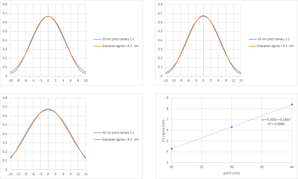
To quantitatively assess the impact of blur, it is most convenient to first fit images of interest with Gaussian curves. In Figure 1, dense line pitches of 20 nm, 30 nm, and 40 nm were fit with Gaussian curves with sigma=4.3 nm, 6.3 nm, and 8.4 nm, respectively. The fitting sigma is found to be excellently fit as a linear function of pitch.
Figure 1. Gaussian fits to dense line images from 20 nm to 40 nm pitch.
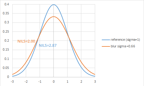
The blur is itself modeled as a Gaussian function. The blur function is convolved with the original image function to produced a blurred image curve. The higher the blur sigma, the more the image is changed. The degradation of image quality is quantified by the NILS (Normalized Image Log-Slope) metric. d[log(dose)]/d[x/feature width] at full-width half-maximum (FWHM) value. A NILS value of 2 has a special meaning: a 10% change in dose results in a 10% change in feature width. This can be considered a dividing line between “bad” and “good” images. Figure 2 shows a reference Gaussian and the effect of blurring with another Gaussian whose sigma is 0.66x the reference sigma (taken to be 1).
Figure 2. The image is degraded to borderline case (NILS=2) by a blur value of 0.66 times the original image sigma.
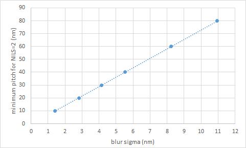
Combining the results of Figure 1 and 2, it is found that for a given pitch, the maximum allowed blur sigma is 0.14x pitch in the 20-40 nm pitch range. Conversely, the minimum pitch for a given resist would be given by blur/0.14. For example, a 5 nm blur sigma would limit resolution to 36 nm pitch.
Figure 3. Minimum dense line pitch (at which NILS=2) as a function of blur sigma.
The most important point to take away from this is that resist blur, which is not directly related to wavelength, is becoming the key factor in determining resolution. The electron blur is itself not easily pinned down, and contributes to the stochastic nature of EUV lithography.
References
[1] K. Eguchi et al., “0.5µm Lithography Using A G-Line Stepper With A 0.6 Numerical Aperture Lens,” Proc. SPIE 0922 (1988).
[2] K-Y. Kim et al., “Implementation of I-line lithography to 0.30 tm design rules,” Proc. SPIE 2440, 76 (1995).
[3] https://www.laserfocusworld.com/optics/article/16556523/challenges-remain-for-157nm-lithography
[4] https://www.spiedigitallibrary.org/journals/journal-of-micro-nanopatterning-materials-and-metrology/volume-20/issue-03/033801/EUV-induced-hydrogen-plasma–pulsed-mode-operation-and-confinement/10.1117/1.JMM.20.3.033801.full
[5] G. M. Gallatin, “Resist Blur and Line Edge Roughness,” Proc. SPIE 5754 (2005).
[6] T. Kozawa and S. Tagawa, “Normalized Image Log Slope with Secondary Electron Migration Effect in Chemically Amplified Extreme Ultraviolet Resists,” Appl. Phys. Exp. 2, 095004 (2009).
[7] R. Gronheid et al., “EUV Secondary Electron Blur at the 22 nm Half Pitch Node,” Proc. SPIE 7969, 796904 (2011).
[8] A. Chunder et al., “Separating the optical contribution to line edge roughness of EUV lithography using stochastic simulations,” Proc. SPIE 10146, 101460B (2017).
[9] Z. Belete et al., “Stochastic simulation and calibration of organometallic photoresists for extreme ultraviolet lithography,” J. Micro/Nanopattern. Mater. Metrol. 20, 014801 (2021).
Share this post via:


Musk’s Orbital Compute Vision: TERAFAB and the End of the Terrestrial Data Center