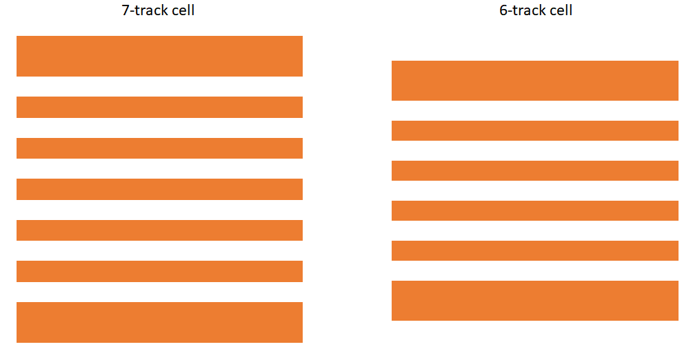
For the 10nm – 5nm nodes, the leading-edge foundries are designing cells which utilize 6 or 7 metal tracks, entailing a wide metal line for every 4 or 5 minimum width lines, respectively (Figure 1).
Figure 1. Left: a 7-track cell. Right: a 6-track cell.
This is a fundamental vulnerability for lithography, as defocus can change the spacing between lines [1], leading to “pitch walking.” This happens when the first and highest orders go out of phase with each other, leading to one diminishing relative to the other. EUV makes things worse by introducing asymmetry between opposite sides of the pupil [2], leading to feature position shift. To get around this, self-aligned patterning is the default alternative. This also offers an exciting opportunity for both 6- and 7-track cells to be produced at the same time on the same chip.
7-track cell process
Targeting a 14-18 nm minimum half-pitch, we expect to use self-aligned quadruple patterning (SAQP) [1]. However, the core features which guide the SAQP consist of unequally sized lines. Specifically, a larger core feature is surrounded by a pair of smaller core features. When patterned lithographically, this also encounters defocus-induced pitch walking. So, it is also preferred to use self-aligned patterning for the core features as well. Self-aligned triple patterning (SATP) [3] naturally can provide the larger feature surrounded by a pair of smaller features. Since the starting pattern is now a single size line/space pattern, there is no threat of pitch walking from defocus. Figure 2 illustrates the self-aligned spacer patterning stages of the process flow for producing the 7-track cell comprising 5 narrow lines surrounded by two wider lines. SATP followed by SAQP (2 x SADP) constitutes self-aligned duodecuple (12x) patterning (SADDP).
Figure 2. Self-aligned spacer patterning stages of the 7-track cell SADDP fabrication process flow. The fourth row indicates the core features for the SAQP stage, consisting of two SADP stages. For self-aligned cutting or blocking purposes, the finally patterned lines are assigned a red or blue color, depending on whether they are on the final spacer interior or exterior, respectively.
6-track cell process
SATP can also produce the SAQP core features for the 6-track cell process (Figure 3) for the same design rules. The main difference is that the SATP starting pitch is 22 times the minimum linewidth or half-pitch instead of 26 times in the 7-track case. With only a ~15% pitch difference, both cases can be patterned using SATP at the same time.
Figure 3. Self-aligned spacer patterning stages of the 6-track cell SADDP fabrication process flow. As in Figure 2, the fourth row indicates the core features for the SAQP stage, consisting of two SADP stages. For self-aligned cutting or blocking purposes, the finally patterned lines are assigned a red or blue color, depending on whether they are on the final spacer interior or exterior, respectively.
Note that the SAQP core features are different from the arrangement that was presented in [4], since it does not use lithographic patterning but SATP. The advantage is that self-aligned line cutting is more effective.
Self-aligned line cutting or blocking
For both the 6-track and 7-track cases presented here, alternate lines, whether wider or narrower, can be assigned to one of two selectively etchable groups (indicated by the red or blue color), depending on whether the location is on the interior or the exterior of the spacers. This is advantageous for patterning line breaks, or cuts (blocks); neighboring lines will not be damaged by cut (block) placement error from overlay. The 6-track cell here maintains this advantage over that shown in [4], where some pairs of adjacent lines from the spacer interiors may still be simultaneously etched.
Pitch walking revisited
The SADDP sequence is essentially four successive SADP stages. Pitch walking will be determined mainly by the spacer deposition thickness control. In the best case, it can be a few to several percent [5,6]. If the spacer exterior is uncovered, it is also subject to etch thinning, which can also lead to pitch walking. This can be addressed by covering the exterior with another deposited layer, against which the spacer etch is selective [7].
Conclusion
The SADDP scheme is an extremely attractive and powerful approach for patterning 6-track and 7-track standard cells for the leading-edge technology nodes. It is currently the only presented approach where the track lithography is free from pitch walking and self-aligned cutting is also conveniently supported.
References
[1] https://www.linkedin.com/pulse/application-specific-lithography-5nm-6-track-cell-frederick-chen
[2] J. Finders et al., Proc. SPIE 9776, 97761P (2016).
[3] US Patent 7807575, assigned to Micron, filed Nov. 29, 2006.
[4] J. U. Lee et al., Proc. SPIE 10962, 109620N (2019).
[5] https://applied-multilayers.com/wp-content/uploads/2017/05/PECVD-DLC.pdf
[6] https://www.researchgate.net/publication/229964576_Film_Uniformity_in_Atomic_Layer_Deposition
[7] US Patent 7732341, assigned to Samsung, filed Mar. 23, 2007.
Share this post via:


Chemical Origins of Environmental Modifications to MOR Lithographic Chemistry