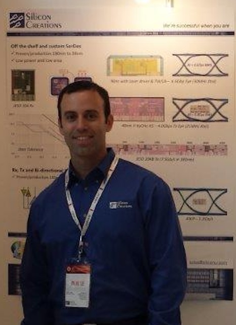
For the next installment in our series of semiconductor CEO interviews we meet with Randy Caplan from Silicon Creations. Randy has helped build the company from a small startup to one of the world’s leading providers of interface and clocking IP. Almost every new chip developed these days has a requirement for PLLs and SerDes. Since many products are differentiated by these blocks, this discussion should provide good insight into some key factors affecting chip performance.
Why are PLLs and SerDes so important in chip design?
As technology evolves, the requirements for faster data processing and increased throughput are growing rapidly. At the same time, demands for reduced power consumption, smaller silicon die area, and shortened product development cycles are putting pressure on designers just to keep chip performance the same.
PLLs generate the high speed clocks that are the heart of every digital design. Improving clock quality in digital designs increases timing margin, allowing more information to be processed in a given time. For data converters, higher resolution and faster conversion rates can be achieved. High speed interfaces also benefit from improved PLL performance.
For SerDes, the increased demand for data throughput is becoming a limiting factor in both system performance and power consumption. The characteristics of transmission materials such as FR4 are not changing, so on-chip techniques must advance as data rate requirements grow. When single lane bandwidth limits are reached, parallel channels must be added, making the power and area of the SerDes a larger percentage of the overall SoC. Since data rate and clock quality are typically defined by the interface standard, area and power of the SerDes quickly become a dominant consideration as more channels are added.
Silicon Creations has grown from a small design service company to providing IP to most of the major chip companies in the world. What’s the secret?
There are many factors, but I think one of the biggest is the way we engage with our customers. We consider ourselves part of the customer’s team, as opposed to an outsider just trying to hand off a black box design. Our primary goal is always success of the customers’ chip. I think this mindset leads to more open communication, resulting in potential issues being resolved early in the design cycle rather than after the silicon comes back, when it’s costly to make changes.
We’ve been fortunate to have assembled a team of talented engineers who created innovative new designs, with performance often far exceeding industry standards. At the same time, we’re aware of the limitations of each design, and go to great lengths to make sure what we promise is what our customers achieve. Many of our customers are shipping hundreds of millions of chips that rely on our PLL and SerDes to function properly. Therefore, better than six sigma quality is often required when considering the joint probability of failure from all the blocks on a complex SoC. We’ve implemented processes and methods that ensure our designs meet these high statistical reliability standards, and our customers know this.
Does your business focus on any particular market segments?
In some ways our business is a proxy for the semiconductor market as a whole, since almost every chip requires a PLL and most require SerDes. Historically, our sales have been distributed across markets in similar proportion to overall chip development.
Over the past several years we’ve seen large growth in the consumer markets, mainly driven by cell phone sales. Our track record of reliability in high volume production has made us a preferred vendor for many of the leading smartphone providers. Home electronics such as flat panel displays and networking have also been big markets for us.
The growth of IoT in the past couple years has influenced us as well. We have several products optimized for ultra-low power applications, including PLLs that consume less than 4µW and still meet very aggressive requirements for clock quality.
To support the new developments in smart cars and automotive electronics, we are partnering with several of the leading foundries to develop and validate a full line of PLL and SerDes products compliant with ISO-9001, ASIL and ISO-26262 Functional Safety standards. Some of our customers are already shipping fully qualified chips for automotive applications.
With so many different semiconductor foundries, geometries, and process flavors, how do you decide process nodes to port your designs to?
In a similar way to how our business mirrors the distribution of various market segments, our IP development scales proportionally to process volume. We’ve worked with nearly every major foundry, in almost all transistor geometries from 350nm down to 7nm, and most with multiple process flavors (low power, high performance, etc.). All in all, we’ve supported well over 100 process variants!
The key for us has been a robust porting flow, based on an internally developed PDK that can be quickly mapped from one process to another. All we need from the foundry is a reasonably accurate simulation model and a DRC deck, and we can deliver a design that works the first time. This has led to ports yielding in processes very early in their life cycle – well prior to their release to ASIC customers.
Our highest production volumes are in 28nm, with over 100 chips using our IP, and millions of wafers shipped. From a product perspective, we have over 300 unique products distributed in approximately equal amounts between 7nm-16nm, 28nm, 40/45nm, 55/65nm, and 80nm-350nm.
So many IP vendors offer PLLs and SerDes. How are you differentiated?
The semiconductor IP market has grown significantly since we started ten years ago, and many companies are now offering quality products for high performance clocking and high speed interfaces. Some may offer a competing product in one case, but could be our partner in another where our products complement each other. We have the highest respect for these companies.
Many times our customers choose our IP because it has the best performance specifications available, because it’s stable in high volume production, or because we can customize a design on an aggressive schedule.
We also offer highly programmable designs that can be digitally configured to work optimally in multiple applications, which adds a lot of value for those developing complex SoCs with many different functions. For example, one customer had a chip with our fractional PLL instantiated 17 times generating all on-chip clocks for applications ranging from ARM core clocking, to PHY reference clocks including Ethernet and PCIe. Another example is our multi-protocol SerDes which is compatible with over 50 different interface standards, with minimal power and area overhead compared to dedicated PHY. Not only is this programmability cost effective by allowing one IP to be used for multiple applications, it allows new applications to be prototyped with existing silicon, simply by reconfiguring the design.
Based on feedback I’ve received from many of our repeat customers, I can also say that our close involvement with customer design teams, our commitment to their success, flexibility to adjust when unexpected changes occur, consistency with meeting schedules, and ability to accurately forecast silicon performance are all key factors in choosing our IP versus other similarly specified products.
What are the challenges facing analog IP providers today?
The pressure to achieve first-time working silicon is immense and growing. Standards for quality (like the ISO26262 Automotive safety standard) deeply constrain what we do, and immense production volumes and short times to market of our products demand designs that yield first time, every time. IP providers don’t get do-overs.
Wafer processes have become much more complicated and process controls are improving but not as fast as the devices get smaller. This means that even modest analog designs have become more complicated and arduous to design, and often times digital control and calibration is necessary. Whereas a few years ago single designers could make a whole chip, teamwork is now necessary for most circuits and the team often includes customers or even competitors. Designers have to be good communicators and have had to learn to write software to do their jobs. This makes solid training essential.
Silicon Creations is now completing its tenth year. Where do you see the company ten years from now?
I expect we will continue to see increasing growth for the foreseeable future. We’ve built a strong base of repeat customers and are regularly adding new ones. The reputation we’ve earned for delivering quality products and world class support makes us a top choice for those selecting IP for their new projects.
The company is privately held and self-funded, so we have the luxury of defining our own path without outside pressure from investors. We’ve built a culture where our employees are excited about the projects they’re working on and about the company’s future. This culture is part of our company’s core, and will be a solid foundation for future growth.
The opportunities we see ahead seem almost unlimited. We hope in the next ten years to take advantage of as many of these opportunities as possible, while continuing to maintain our high standards for product quality, customer support, and quality of life for our employees.
How will Silicon Creations help to address the requirements for next generation clocking and interface IP?
We continue to exploit the performance advantages of each new process technology, as well as innovating to optimize design architectures for improved figure of merit (lower power and area for a given data rate). Our SerDes products are currently being used in applications requiring up to 20Gb/s, with power per lane below 5mW/Gbps for short reach and below 8.5mW/Gbps for long reach. We will soon be extending this to 28Gb/s and beyond, with further optimization in power an area.
Our PLL specifications define the state of the art in performance / power / area figure of merit. We continue to extend this through an active research and development program, and expect to extend what’s possible in on-chip clock generation with new PLL architectures as well as continual optimization of our existing ones. It is becoming more and more frequent that our customers replace discrete clocking ICs in their systems with our fully integrated solutions.
We are constantly looking for ways to push the limits of what’s possible in semiconductor technology. Each time we take a step forward in the performance of our IP, our customers are enabled to also push the limits of their technology, which in turn encourages us to push further. I think it is this iterative push towards progress that will enable the next generation of technology.
You can read more about Silicon Creations HERE.
Also Read:
Expert Interview: Rajeev Madhavan
CEO interview: Rene Donkers of Fractal Technologies
CEO Interview: Albert Li of Platform DA
Share this post via:


Comments
There are no comments yet.
You must register or log in to view/post comments.