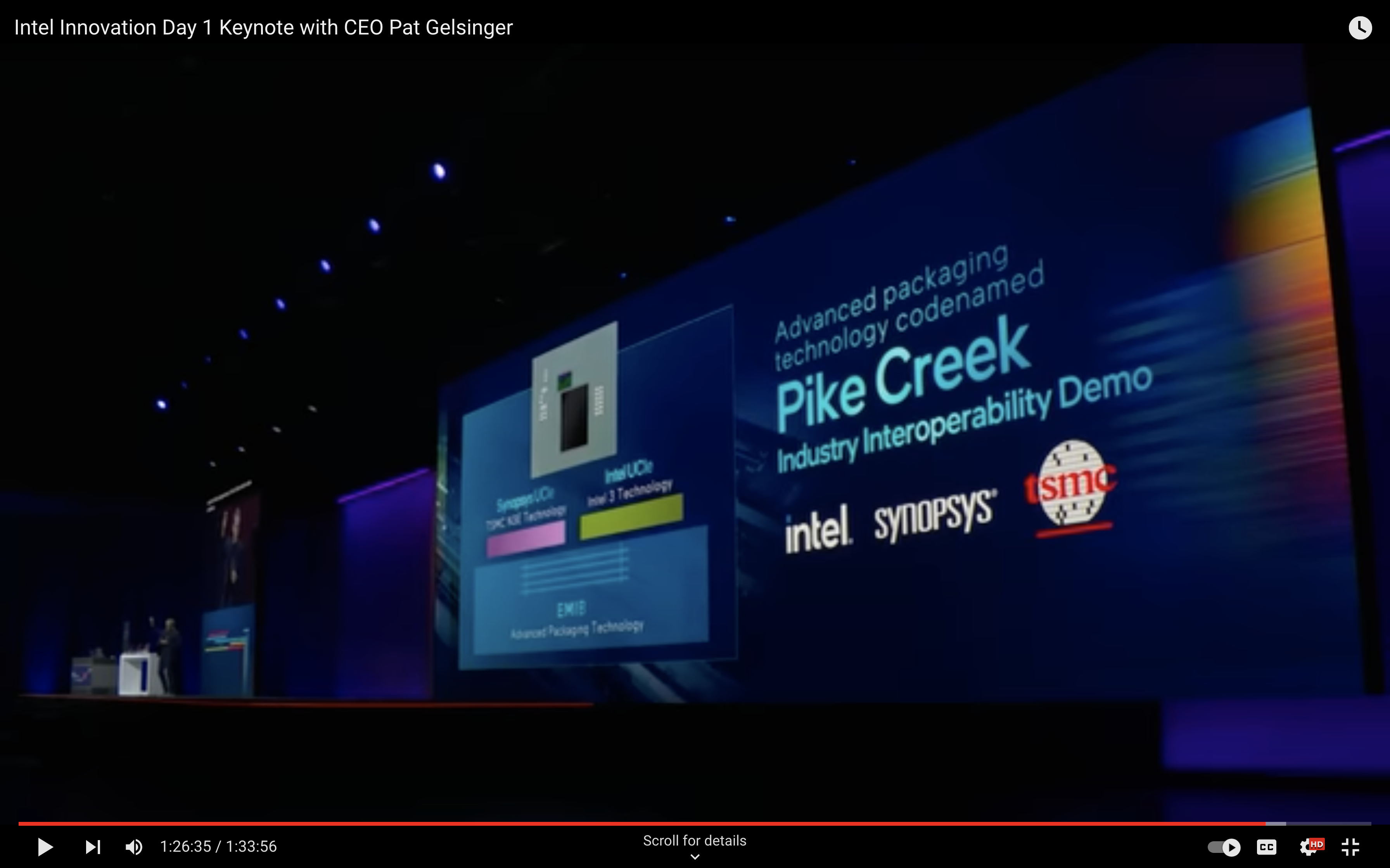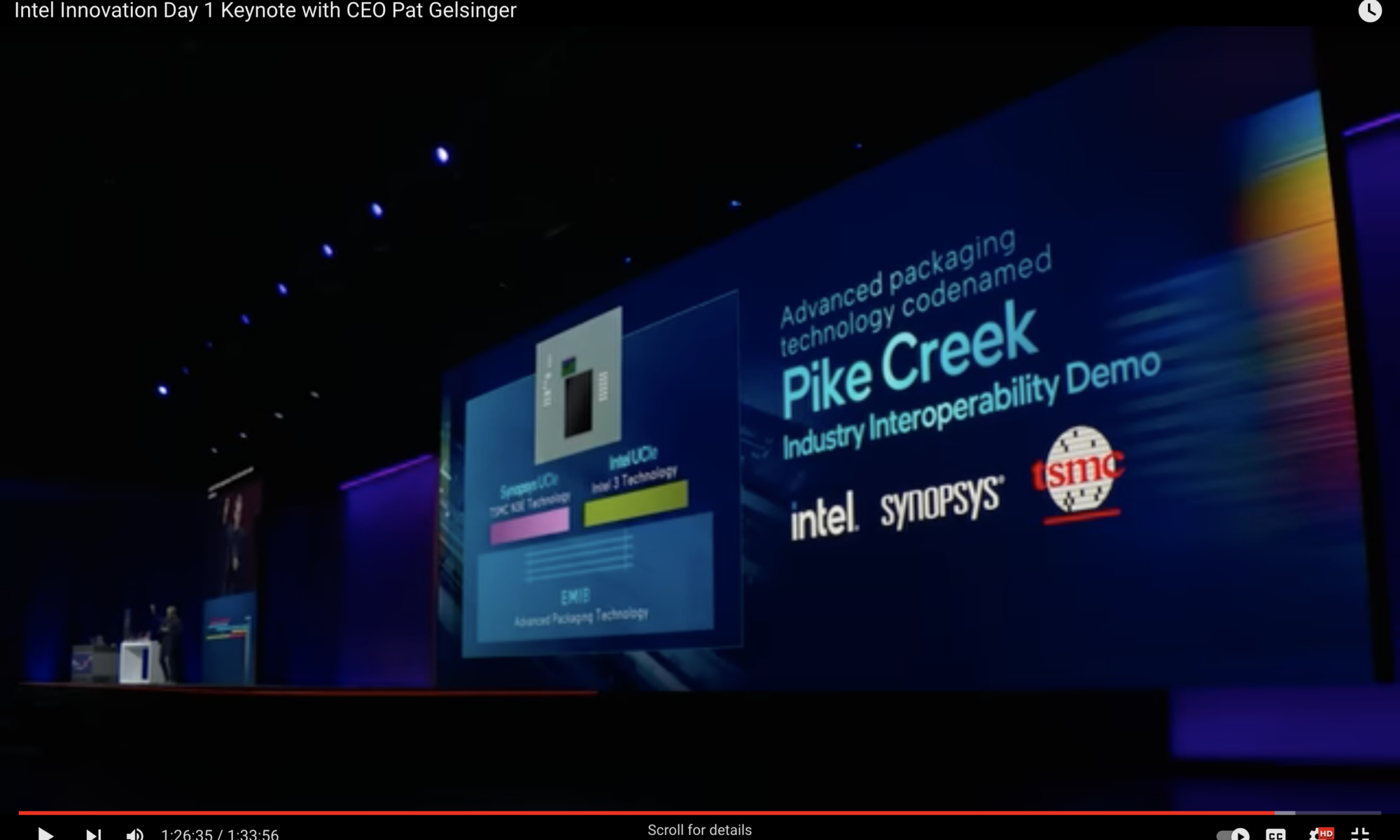
Intel recently made headlines when CEO Pat Gelsinger unveiled the world’s first UCIe interoperability test chip demo at Innovation 2023. The test chip built using advanced packaging technology is codenamed Pike Creek and is used to demonstrate interoperability across chiplets designed by Intel and Synopsys. More details on this later in this writeup. This announcement marked a critical milestone in the journey toward an open and interoperable chiplet ecosystem and highlights the UCIe standard’s commitment to driving the chiplet revolution forward.
Proofpoint of UCIe InterOp
The significance of Intel’s announcement lies in its emphasis on interoperability—the ability of chiplets to communicate seamlessly and effectively, regardless of origin. The announcement marks the public debut of functioning UCIe-enabled silicon, featuring an Intel UCIe IP manufactured on Intel 3 process node and a Synopsys UCIe IP fabricated on the advanced TSMC N3E process node. These two chiplets in the Pike Creek test chip communicate via Intel’s EMIB interconnect bridge, ushering in a new era of heterogeneous chiplet technology.
The Pike Creek test chip serves as a tangible demonstration of UCIe’s capabilities, showcasing how chiplets from different vendors can work together efficiently within a single system. Intel has announced plans to transition from proprietary interface to the UCIe interface on its next-generation Arrow Lake consumer processors. This demonstrates Intel’s commitment to fostering an open, standardized ecosystem for chiplets and aligning with the industry’s shift towards UCIe.
The Backdrop
In recent years, industry leaders such as Intel, AMD, NVIDIA and others have embraced chiplet-based multi-die systems—an innovative approach that involves integrating small, specialized, heterogeneous or homogeneous dies (or chiplets) into a single package. However, the predominant focus has been on of captive systems, where all chiplets within a package are developed by the same vendor. However, this approach limits innovation that arises from incorporating specialized chiplets from different sources.
Heterogeneous integration offers the potential for more versatile and powerful systems by allowing chiplets from various vendors to seamlessly work together in a multi-die system. To fully unlock the potential of chiplet-based multi-die systems, the industry recognizes the imperative of heterogeneous integration. The success of a chiplet-based industry in turn depends heavily on encouraging a broad base of vendors to enter and grow an open chiplet ecosystem. But without a standardized interface for chiplet-to-chiplet communication, integrating chiplets from different vendors becomes complex. Interoperability (InterOp), the seamless communication between chiplets regardless of their origin, stands as a central goal for realizing the full potential of heterogeneous chiplet integration.
Heterogeneous Interoperability is Key
Addressing the heterogeneous interoperability need, the Universal Chiplet Interconnect Express (UCIe) standard was introduced in 2022 through a consortium. With promoter members such as Intel, AMD, TSMC and others and contributor members such as Synopsys, Amkor, Keysight and many others, the consortium is now 120+ members strong. Developed collaboratively by major players in the semiconductor industry, the UCIe standard aims to provide an open-source interface for chiplet interconnects interoperability. By standardizing communication between chiplets, UCIe not only simplifies the integration process but also fosters a broader ecosystem where chiplets from different vendors can seamlessly be incorporated into a single design.
Benefits of UCIe
UCIe consortium members have set ambitious performance and area targets for the technology. By categorizing target markets into two broad ranges with standard 2D packaging techniques and advanced 2.5D techniques, UCIe offers versatility in meeting the diverse needs of chip designers. Advanced 2.5D techniques include technologies such as Intel’s Embedded Multi-Die Interconnect Bridge (EMIB) and TSMC’s Chip-in-Wafer-on-Substrate (CoWoS). Chipmakers can select chiplets from various designers and seamlessly incorporate them into new projects, significantly reducing design and validation work. UCIe allows designers and manufacturers to select chiplets based on their specific requirements, enabling a more flexible and diverse approach to semiconductor design.
In essence, UCIe helps accelerate time-to-market, reduce development costs, promotes innovation, broadens supplier base and enhances overall product development efficiency. Support for 3D packaging is on the roadmap.
Summary
As the semiconductor industry moves forward, the implications of UCIe are profound. The standard not only propels chiplet technology into the era of heterogeneous integration but also opens doors to a new wave of innovation. With a standardized interface in place, chip designers can mix and match chiplets with confidence, creating tailored solutions for a wide range of applications. For example, the potential for heterogeneous chiplets integration opportunities in the automotive market is tremendous. The UCIe consortium recently announced the UCIe 1.1 specification to deliver valuable improvements in the chiplet ecosystem, extending reliability mechanisms to more protocols and supporting broader usage models. Enhancements for automotive usages include predictive failure analysis and health monitoring and enabling lower-cost packaging implementations.
Synopsys
As the leader in EDA and semiconductor IP, Synopsys offers comprehensive solutions to address the ecosystem needs for chiplets integration.
For more details on Synopsys UCIe IP, visit Synopsys UCIe IP Solutions.
Also Read:
Synopsys.ai Ups the AI Ante with Copilot
Synopsys 224G SerDes IP’s Extensive Ecosystem Interoperability
Synopsys Debuts RISC-V IP Product Families
Share this post via:


Comments
There are no comments yet.
You must register or log in to view/post comments.