In a simple answer – everyone. A keynote presentation “Sensing the Unknowns and Managing Power” by Mahesh Tirupattur, the Executive Vice President at Analog Bits at the recent Siemens User2User conference, discussed the need and application of sensors in computing and power applications. Why sense? As Mahesh explains, sensing provides the middle ground between the pure analog functions and the digital systems. The need for sensing is everywhere, and in today’s latest system-on-chip designs the challenges start with the doubling of performance while halving the power consumption. With that comes the integration of billions of transistors and if any one component fails, the entire SOC could fail. Those challenges escalate with the use of FINFET transistors due to their exacting manufacturing requirements.

Challenges with such a design include the difficulties of exhaustively verifying the design before tape-out as well dealing with an almost infinite range of manufacturing variations. Additional issues include dealing with dynamic power spikes superimposed on PVT variations in mission mode. Large die sizes with multiple cores can also cause significant local temperature variations of 10 to 15 degrees across the die, and sensing can quickly detect and take corrective actions, such as software load balancing. Process variations can also be detected through the use of multiple Vt devices. Power distribution and power-supply integrity are also challenges for large chips and sensing can monitor and take instantaneous corrective actions at high processing speeds. With large numbers of processing cores on a chip, dynamic current surges can cause internal voltages to exceed functional limits.
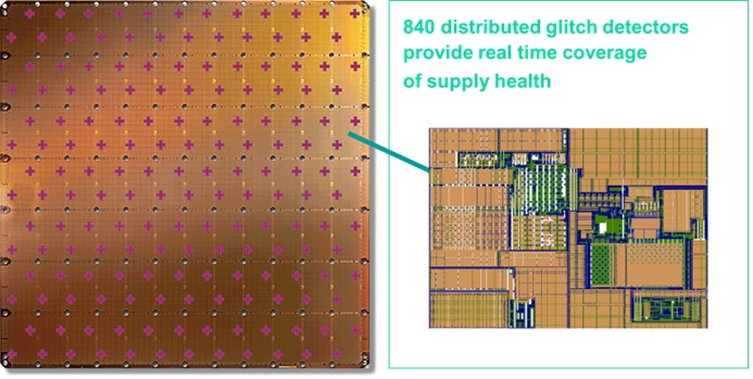
As an example, Mahesh examines the design of the world’s largest AI chip, the Cerebras WSE-2. This wafer-sized “chip” has an area of 46,225 mm2 and contains 2.6 trillion transistors, trillions of wires, and 850,000 AI optimized compute cores (see the photo). Fabricated using TSMC’s 7 nm process technology, the device also contains 40 Gbytes of on-chip memory and delivers a 220 Petabit/s fabric bandwidth. Multiple sensors are embedded on the wafer – 840 glitch detectors and PVT sensors designed by Analog Bits provide real-time coverage of supply health, monitoring functional voltage and temperature limits.
The sensors can detect anomalies with significantly higher bandwidth than other solutions that miss short-duration events. Able to provide high-precision real-time power-supply monitoring exceeding 5 pVs sensitivity, the sensor intellectual property (IP) blocks are highly user programmable for trigger voltages/temperature, depth of glitch and time-span of the glitches. The ability to monitor multiple thresholds simultaneously provides designers and system monitors with a wealth of data to optimize the instantaneous current spikes suppression and overall effectiveness. Additionally, the fully-integrated analog macro can directly interface to the digital environment, can be abutted for multiple value monitoring and packs an integrated voltage reference.
Mahesh also sees the need for other power related sensors – on-die PVT sensors with accuracies trimmable to within +/-1C, integrated power-on-reset sensors that detect power stability in both core circuits and I/O circuits, and also offer brown-out detection. These sensors are just one piece of the puzzle that IP designers are facing. We have to design a test chip in a brand new process—it takes us several months to do the design and about nine months to get the test chip back from the fab. Then it may take a year or more for the customer to incorporate the IP in their design. As an IP company our challenges are even greater—customers are not just designing a chip, but designing a system, and that means that they have to co-optimize everything together. Thus, monitoring power is not just the power as a single chip, but power as an entire system and there comes the challenges of voltage spikes and power integrity and those issues, if not sensed and dealt with, can basically kill the whole system. Thus monitoring the thresholds and spikes, and quickly responding to the issues can result in more reliable systems.
In addition to power-related IP blocks, Analog Bits also developed a “pinless” phase-locked loop (PLL) that solves some of the on-chip clocking issues. The PLL can be powered by the SOC’s core voltage rather than requiring a separate supply pin. That reduces system bill of materials costs by eliminating filters and pins, and the IP can be placed anywhere without and power pad bump restrictions. Last but not least, Analog Bits also has family of SERDES IP blocks that are optimized for high-performance, low-power SOC applications. The IP blocks are available in over 200 different process nodes, including 5 nm (silicon proven), 4 nm, and 3 nm (both in tape out), as well as older nodes, from all major foundries.
Also read:
Analog Bits and SEMIFIVE is a Really Big Deal
Low Power High Performance PCIe SerDes IP for Samsung Silicon
On-Chip Sensors Discussed at TSMC OIP
Share this post via:


Comments
There are no comments yet.
You must register or log in to view/post comments.