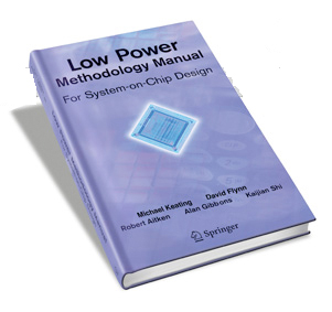
There was recently a forum discussion about the best low power techniques. Not surprisingly we didn’t come up with a new technique nobody had ever thought of but it was an interesting discussion.
 First there are the techniques that by now have become standard. If anyone wants more details on these then two good resources are the Synopsys Lower Power Methodology Manual (LPMM) and the Cadence/Si2 Practical Guide to Low Power Design. The first emphasizes UPF and the second CPF but there is a wealth of background information in both books that isn’t especially tied to either power format.
- Clock gating
- Multiple Vt devices
- Back/forward biasing of devices
- Power gating for shutdown
- State retention
- Multi-voltage supplies
- Dynamic voltage scaling
- Dynamic frequency scaling (Dynamic Voltage and Frequency Scaling – DVFS)
A lot can be done at the system/architectural level, essentially controlling chip level power functionality from the embedded software, such as powering down the transmit/receive logic in a cell-phone when no call is taking place.
 Asynchronous logic offers potential for power saving, especially for the ability to take silicon variation in the form of lower power as opposed to binning for higher performance. After all, 30% of many SoCs power budget is consumed by the clock itself. But there are huge problems with the asynchronous design flow since synthesis, static timing, timing driven place & route, scan-test etc are all inherently built on a synchronous model and break down when there is no clock. These are soluble problems if enough people wanted to use asynchronous approaches, but a lot of tools need to be fixed all at once (but to be fair, this was the case with the introductions of CPF and UPF too). But definitely it has a feel of “you just have to boil the ocean.”
WIth more powerful tools, such as those from Calypto, more clock gating can be done than the simple cases that synthesis handles (replacing muxes recirculating values with a clock gating cell). If a register doesn’t change on this clock cycle, then the downstream register won’t change on the next clock cycle. Some datapaths have a surprising amount of these sorts of structures that can be optimized, although the actual power savings are usually data dependent.
As we have gone down through the process nodes, leakage power has gone from an insignificant part of total power dissipation to being over half in some chips. Some of the new Finfet transistor approaches look like they will have a big positive effect on leakage power too, but there is a lot that can be done with any process using libraries containing both low-leakage and high-performance cells and using the high-performance cells only on the most critical paths.
The real bottom line is that power requires attention at all levels. The embedded software ‘knows’ a lot about which parts of the chip are needed and when. For example, the iPad supposedly has multiple clock rates for the A5 chip and only goes up to the full 1 GHz when that performance is needed for CPU intensive operations. Architectural level techniques such as choice of IP blocks can have a major impact. Low power synthesis is with clock gating and multiple libraries. Circuit design techniques. And finally process innovation that keeps the power under control as the transistors get smaller and smaller.


Musk’s Orbital Compute Vision: TERAFAB and the End of the Terrestrial Data Center