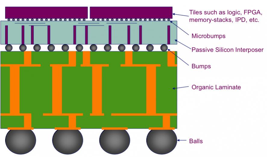
 Have you ever had the experience where you look up some unusual word in the dictionary since you don’t remember seeing it before. And then, in the next few weeks you keep coming across it. Twice in the last week I have been in presentations about the economics of putting die onto silicon interposers and the possibility of a new ecosystem growing up of bare microbumped die being available as a way of putting systems together. Sort of bringing multi-chip modules into the next generation.
The first was a presentation by Javier de la Cruz of eSilicon’s packaging department at the GSA 3D IC meeting. OK, so at a 3D IC meeting it is hardly news that someone was talking about silicon interposers. But he started from the basic economics that the increasing cost per tapeout drives down the number of tapeouts (there are other factors too, like the increasingly large volume needed to justify doing a state-of-the-art SoC). So there has to be another way to get custom hardware.
The other presentation was by Ivo Bolsens, the CTO of Xilinx. Obviously one of the ways to get custom hardware is to use an FPGA but in fact that was not what Ivo was talking about. He was talking about what he calls “crossover” ICs that combine features of ASICs, ASSPs and FPGAs. One way to do that is to create a tightly integrated processor subsystem combining processors, memories, some peripherals and FPGA fabric on one die. But the other way is to put separate die onto a silicon interposer.
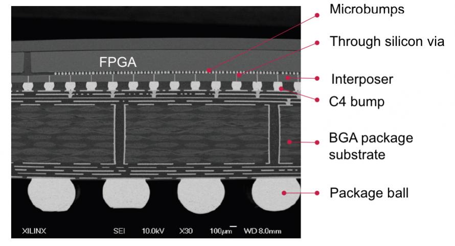 Xilinx has been a leader in silicon interposer, using the approach to create large designs in new process nodes and get high yield. Xilinx calls this “more than Moore” approach “stacked silicon interconnect technology.” For the Virtex-7, instead of building a huge 28nm FPGA in a single die that would yield unacceptably, they put quarter array 28nm slices onto a 65nm silicon interposer (with tens of thousands of connections between the slices, this is not your father’s multi-chip Oldsmobile). See photomicrograph of a cross section to the left.
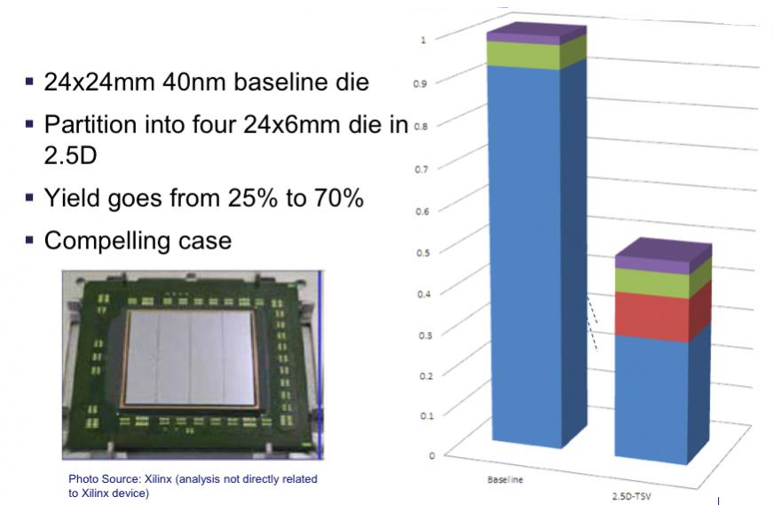 Interestingly, eSilicon had taken their yield models and analyzed a Virtex-7-like design and confirmed that by their numbers (they had no access to any internal Xilinx data) they were making a big saving. eSilicon estimated that in a 40nm process 24mm by 24mm baseline die compared to partitioning into four 24mm by 6mm die that the yield would go from 25% to 70%. Even with the additional cost of the interposer the cost saving looks to be over 50%. Pretty compelling. And Xilinx is actually at 28nm where the immaturity of the process should yield still more dramatic yield increase.
eSilicon has an approach that they call MoZAIC to allow them to put designs like this onto interposers to reduce the cost. There are three economic drivers that make this cost-effective: with pad limited die the interposer can fan out the I/O in a cheaper process, instead of building a large die in a very expensive process. Wth regular structures the partitioning can increase yield, as in the Xilinx case. And thirdly, it is possible to mix multiple technologies such as RF, FPGA, analog etc on a single interposer.
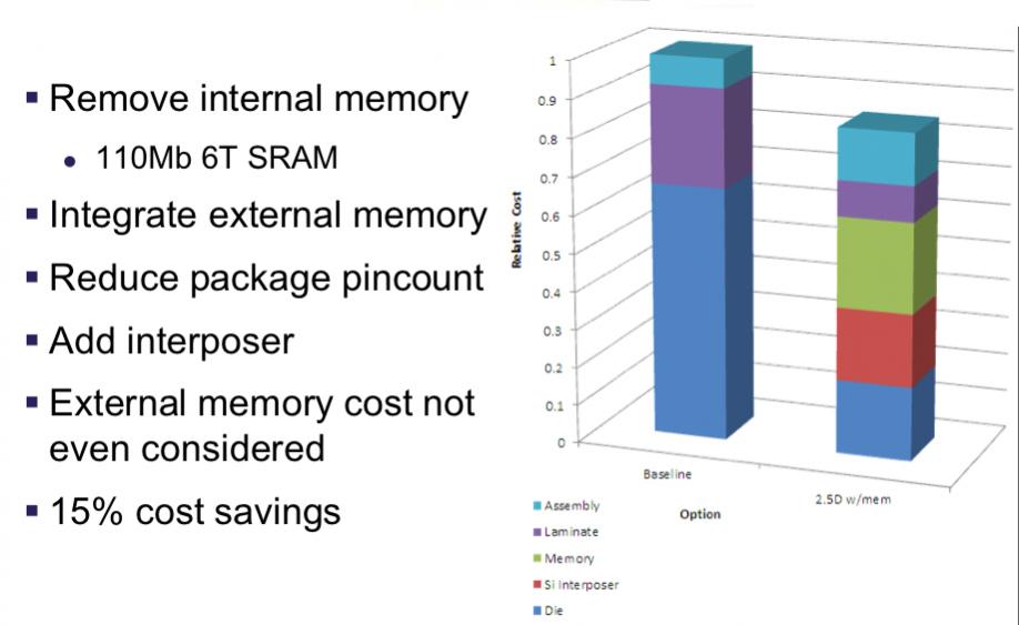 In the designs eSilicon had considered, some had negligible cost-savings and, in some cases, costs would increase. But some were very compelling. For example, one design contained 110Mb of 6-transistor SRAM plus more off-chip memory. By using an interposer, they could reduce the pincount (no external memory), remove the SRAM from the SoC, integrate the external memory onto the interposer and get a cost saving of 15% even without counting any saving due to no longer needing external memory on the board.
But the real attraction of this approach, that both Xilinx and eSilicon talked about, is if an ecosystem comes into existence where standard tiles are available to go along with custom tiles.
Two sweet spot customers for this approach could be mobile and networking. Mobile wants the lowest power and the smallest physical package, so integrating separate packages (e.g. radios etc) onto a single interposer has big potential gains. I know from a talk at the last DAC that Qualcomm for one is looking at this sort of approach. For networking, there are big limits on I/O count and huge difficulty (technical, power, testing) in using those limited pins to multiplex access to memory using DDR4/5. But with an interposer, very wide memory access is possible so complex memory controllers are not required.
Xilinx also see this as a attractive way to put CPU, memory and programmable logic into the same package, and with a lot more flexibility than the alternative where everything is integrated onto a single die with a single compromise on the amount of memory, programmable logic, number of cores and so on. I know from VLSI days years ago that putting memory onto a gate-array was really difficult because there was either too much memory or too many gates. If you did a custom base then you lost a lot of the advantages of gate-array that they could be turned quickly by pulling uncommitted arrays from wafer bank and adding the metal. It is easier to waste silicon now (and FPGAs are, by definition, wasting silicon for flexibility) but the same problem of finding the sweet spot exists.
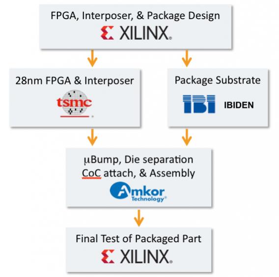 eSilicon has started a prototype design to tape out this year to pipeclean the methodology. They have selected the partners for tiles (memory, IPD, FPGA, microprocessor, PHY), the tools, the IP, assembly and test partners. Xilinx are obviously ahead in this game, at least for the Virtex-7. It is worth noting that there is a lot of novel stuff in putting a design like this together. The interposer has through-silicon-vias (TSVs) and so has to be very thin, making it too fragile to handle as a wafer without attaching it to another piece of silicon or glass, which has to eventually be removed. There are many additional test issues since the tiles need to be tested (and tested well since a tile that slips through test onto the interposer results in discarding a lot of good tiles too). Then the final assembled system needs to be tested which requires careful thought about test architecture so that all the tiles can be accessed from external pins even if they are actually only connected internally to other tiles.


Musk’s Orbital Compute Vision: TERAFAB and the End of the Terrestrial Data Center