2019 will be a big year for PCIe. With the approval of version 0.9 of the Base Layer for PCIe 5.0, implementers have a solid foundation to begin working on designs. PCIe 4.0 was introduced in 2017, before that the previous PCIe 3.0 was introduced in 2010 – ages ago in this industry. In fact, 5.0 is so close on the heels of 4.0, many products may simply leapfrog the 4.0 version and go directly to 5.0. Each version of PCIe has doubled the throughput, with 5.0 coming in at 63 GB/s with a 16 lane implementation. Compare that to the 4 GB/s throughput for the 2003 PCIe 1.0 with 16 lanes.
It’s even more amazing to go back to the specs of the original PCI from Intel in 1992. Back then the clock rate was 33.33 MHz with data rates of 133MB/s for a 32-bit bus. Of course, the original PCI used parallel synchronous data lines, which limited throughput due to clocking and bus arbitration issues. All of the PCIe specifications rely on high speed serial data transfers with each connected device having a dedicated full-duplex pair of transmit and receive lines. As with modern serial links the clock is embedded in the data stream, eliminating the need for external clock lines. Multiple lanes are used to increase throughput with the added requirement of limited lane skew so that the controller can reassemble the striped data.
Indeed, designers of PCIe IP and teams that are integrating PCIe 5.0 need to be mindful of a number of technical considerations. Synopsys recently posted an informative article about PCIe 5.0 on their website that discusses many of these issues. At the rate of 32GT/s the Nyquist frequency increases to 16GHz. This higher frequency for transmitting data complicates the channel design. Insertion loss increases at this higher operating frequency, and cross talk becomes a more serious problem. FR4 as a choice for PCB material is completely ruled out for most designs, unless retimers can be used. Maximum allowed channel loss for PCIe is 36dB. A 16 inch 100 Ohm differential pair stripline on FR4 would have a loss of 33.44 at 16 GHz. Leaving virtually no loss allowable for the other elements of the channel such as packaging, connectors, cabling, etc. Fortunately, there are alternatives that perform better, if the right design decisions are made.
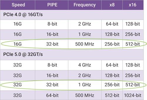
In their article Synopsys also points out that the interplay between the PHY and controller becomes more interesting. There is an interface, known as the PHY Interface for PCIe (PIPE), for integrating the PHY and controller, with the latest PIPE 5.1.1 supporting the changes for PCIe 5.0. In the latest version, the pin count has been reduced by moving side-band pins into register bits, the Physical Coding Sublayer (PCS) moved from the PHY to the controller to permit the use of more general purpose PHY designs, and a 64-bit option has been added to help reduce the speed needed in the PIPE interface.

The Synopsys white paper offers an excellent description of the trade-offs relating to timing closure on 8 and 16 lane interfaces running at the highest transaction rates. Using a 512-bit controller with a 32-bit PIPE, running at 32 GT/s with 16 lanes, the controller logic timing can be closed with a 1 Ghz clock rate. Other options either require much higher clock rates, making timing closure infeasible, or call for a larger controller that is not available in today’s market.
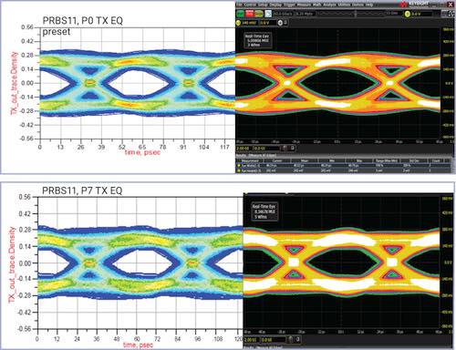
Synopsys also provides a lot of useful information about packaging and signal integrity considerations for PCIe 5.0. They conclude with a section on modeling and testing of the interfaces.

Synopsys offers a complete solution for PCIe 5.0, including controllers, PHYs, and verification IP. This should come as some comfort to design teams that are looking to add the latest generation to their products.
There are a lot of considerations and choices to be made in order to build the right interface for a given application. The Synopsys DesignWare IP for PCIe includes configurability with support for multiple data path widths, including a silicon proven 512-bit architecture. The article on their website is very informative and helps clarify some of the biggest issues relating to the move to PCIe 5.0.
Share this post via:


Comments
There are no comments yet.
You must register or log in to view/post comments.