Discussion on machine learning (ML) and hardware design has been picking up significantly in two fascinating areas: how ML can advance hardware design methods and how hardware design methods can advance building ML systems. Here I’ll talk about the latter, particularly about architecting ML-enabled SoCs. This approach is getting major traction for inferencing applications particularly when driven by power considerations (eg in the IoT and increasingly in automotive apps), also in training when driven by demand for highest performance per Watt (eg Google TPU).
Architecture has to be the center of design in such a system, optimizing the algorithm and architecture for your CNN. For the core algorithm, this has to be in choice of number, types (convolution, pooling, …) and characteristics (stride, …) of layers in the network. In the implementation, memory support is one critical consideration. Neurons like tightly-coupled memories for weights, activation functions and retrieving and storing neuron inputs and outputs, but everything can’t be tightly-coupled so you also need high-bandwidth access to larger memories – like caching but implementation can be quite different in CNNs. And you want to optimize PPA, aggressively if the design is targeted to a battery-operated application.

There are challenges in finding an optimal architecture for these systems. RTL isn’t an option – you need to test out different options with 100’s of MB of data (images as an obvious example) so this has to run at a higher level of abstraction. And it’s not obvious (to me at least) how you would experiment with CNN architectures in a JIT-type virtual-prototype running on a general-purpose processor (or even a cluster). This class of architecture design seems a much better fit with TLM approaches, for example Platform Architect Ultra.
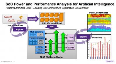
You’ll likely start in one of the standard CNN frameworks (Caffe, TensorFlow, etc) where most experts in the field are familiar with building CNN graphs. You can translate this into a workload model in Platform Architect (Synopsys calls this a task graph). This can then be mapped into an IP in your larger SoC model: CPUs, memory interfaces and on-chip bus. Naturally the platform supports a rich library of IPs and VIPs for this task:
- Processors – Arm, Synopsys ARC, Tensilica and CEVA DSP, traffic generators and more
- Memory subsystem – DDR and multiport memory controllers from Arm and Synopsys
- Interconnect models from Synopsys, Arteris IP, Arm and NetSpeed
Architecting the bulk of the SoC is pretty familiar; what is different here is designing the task graph for the CNN, or adapting it from an imported graph. I don’t want to get too much into the details of exactly how this works – you should follow the webinar link at the end to get a more complete description. But I think it is useful to highlight some of the key points for those of us who think more in terms of conventional logic.
Since you’re likely working with an imported CNN task graph, you probably need to build sub-components which will ultimately connect to TLM models, starting for example with a convolution layer in which you need tasks like read_input (reading an image sub-block), read_coefficients (e.g. for weights), process the neural function and write_result. The tool supports this through creation of a task components as blocks which you then connect to create a graph, indicating serial versus parallel processing. You also add parametrization to tasks and connections for things like height and width of a frame and the stride (how much the filter shifts on the input map per convolution).
You can them simulate this model and sweep over different scenarios, looking at basic latencies and utilization of resources, and fine-tune and connect this as a hierarchical sub-component in the larger task graph. You will also build a structure to support the main body of your SoC (this is standard Platform Architect stuff), into which your CNN task graph is instantiated.
From here you start mapping between tasks and TLM models in the library – connecting your task-graph to a TLM implementation. Now when you simulate with scenarios, you get more realistic info on latency, throughput, utilization and so on. You can also do system-level power analysis at this stage by adding UPF3 power monitors (state machines, bound to each TLM model, with estimated power per state. Ah-hah – so that’s where these UPF3 monitors are used 😎)
The presenters (Malte Doerper – PMM, and Tim Kogel – AE manager, both in the virtual prototyping group) show application of these concepts to an AlexNet case study (AlexNet is the reference CNN benchmark everyone uses). Their goal on starting is to process a frame in 10ms with 4 frames processing in parallel, and to consume less than 500mW. They show a nice analysis, based on running over multiple scenarios where they can compare implementation choices against meeting the performance spec, power and energy (the old trick – run faster, higher power but lower energy). And of course they meet their power and performance goals!
I found this a pretty interesting exposition of how CNN design can fit comfortably into the full SoC architecture goal. Modeling convolution layers through tasks may look a little different, but it all seems to flow quite smoothly into full architecture creation. There’s a lot more detail in the webinar, along with a quite detailed Q&A. You can learn more HERE.
Share this post via:


Comments
There are no comments yet.
You must register or log in to view/post comments.