In the 1970’s, when Moore’s Law was still in its infancy, Bill Lattin from Intel published a landmark paper [1]. In it he identified the need for new design tools and methods to improve layout productivity, which he defined as the drawn and verified number of transistors per day per layout designer. He said existing solutions would simply not keep up with the fabrication process roadmap.
For new design methods, the industry has clearly embraced reuse, from the adoption of cell libraries to complex IP macro functions — that has addressed the “regularization” goal that Lattin described, which he defined astotal devices on chip divided by drawn devices(excluding memories).
For new layout tool capabilities, there have been numerous advances:
- parameterized cells (and related programming languages, data model API’s)
- connectivity-driven layout (derived from the schematic)
- integrated/interactive rule checking
Yet, there clearly remains more to be done.
The complexity of today’s advanced processes have added more physical design requirements which impact performance and manufacturability, from dummy fills to layout-dependent context effects (LDE’s) to multipatterning decomposition — all must be managed as productively as possible.
Electrical analysis closure is becoming increasingly difficult to achieve at advanced process nodes, which necessitates addressing both early identification during implementation and fast iterative methods from the (project time-critical) signoff flows back to physical design.
These challenges in physical and electrical design verification are going to increase in magnitude at newer nodes, with greater reliance upon multipatterning and greater disparity between improved transistor performance and the (scaled) interconnect current densities.
Synopsys has recently announced a new physical design toolset — Custom Compiler — to address these issues in layout design productivity.
I recently had the opportunity to meet with Dave Reed, Director of Marketing, Analog/Mixed-Signal Group, who provided a preview of the tool capabilities. Dave highlighted how the features of Custom Compiler help address the layout productivity issues above:
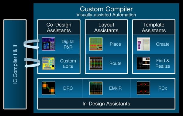
(1) In-Design Assistants for electrical analysis
- addresses the need for early identification of EM and IR issues
- supports color-aware physical/electrical characteristics of interconnects
- applied during physical implementation
(2) a Symbolic Editor for the definition and management of a library of (complex) design templates addresses the need for more reuse of proven layout topologies
(3) device-level place-and-route interactive features, aka Layout Assistants
and
(4) Co-Design integration with IC Compiler/IC Compiler II
Then, we walked through two design scenarios, to demonstrate some of the cool, new features of Custom Compiler.
Despite all the tool capabilities added since Bill Lattin’s presentation, the physical implementation of analog IP has remained a difficult and complex task. Layout designers and schematic designers need to be in full lockstep, with regards to requirements for device matching, layout symmetry, color decomposition, etc.
Consider the relatively simple case of an input differential pair, two transistors with stringent matching requirements to minimize offset. Each transistor has multiple fingers and a multiplicative M factor. (Dave added the constraint that each schematic instance is actually n layout devices in series per finger, to reflect an effective channel length of n*L.) This differential pair needs an interleaved, symmetric layout, from device placement to dummy fill to interconnect routing.
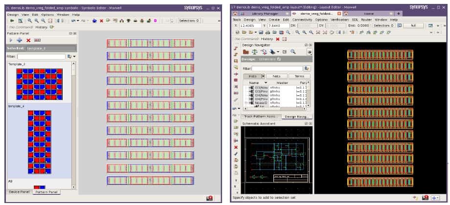
Layout designers can reference the Symbolic Editor in Custom Compiler, to examine if the library of existing templates contains an entry that satisfies the design requirements, or if an entry could be easily adapted to satisfy new constraints (e.g., a different aspect ratio). This is more than simply selecting fixed cells from a library — the Symbolic Editor easily creates new templates, while maintaining the relationship between schematic instances, (multiple) device placements, and total device connectivity.

The figure above illustrates the Symbolic Editor, and how (placed device) templates are identified, with the red/blue colors in the template representing the interleaving A/B devices in the differential pair. Once selected, the template is added into the selection panel of the layout view.
Let’s say a suitable placed differential pair device template was added to the open layout cell — then, the device-level visual Layout Assistant in Custom Compiler is used to route interconnects. As the relationship between devices and their symmetry requirements is understood, multiple routes are auto-generated for related device connections from a single drawn path, as illustrated below. (These routes are symmetric, layer-consistent, and color-aware.)

Next, consider the scenario where an on-chip bus is routed in ICC/ICC II, yet subsequent (signoff) electrical analysis necessitates that the bus be edited — e.g., to fix timing, noise, EM.

As illustrated in the figure above, with Custom Compiler, those custom edits can be implemented and returned back to ICC/ICC II, maintaining full database integrity.
With the introduction of Custom Compiler, Synopsys has clearly focused on adding visual layout design productivity tools, spanning from IP design support to new methodologies for rapidly achieving electrical/physical design closure. Perhaps it’s time to update Lattin’s layout productivity metrics, to something more akin to time to complete a suite of design scenario tasks. In this regard, there are many areas where Custom Compiler would excel.
For additional information, please follow this link.

-chipguy
[1] Bill Lattin, “The Problem of the 80’s for Microprocessor Design”, Caltech Conference on VLSI, 1979.
Share this post via:


Comments
There are no comments yet.
You must register or log in to view/post comments.