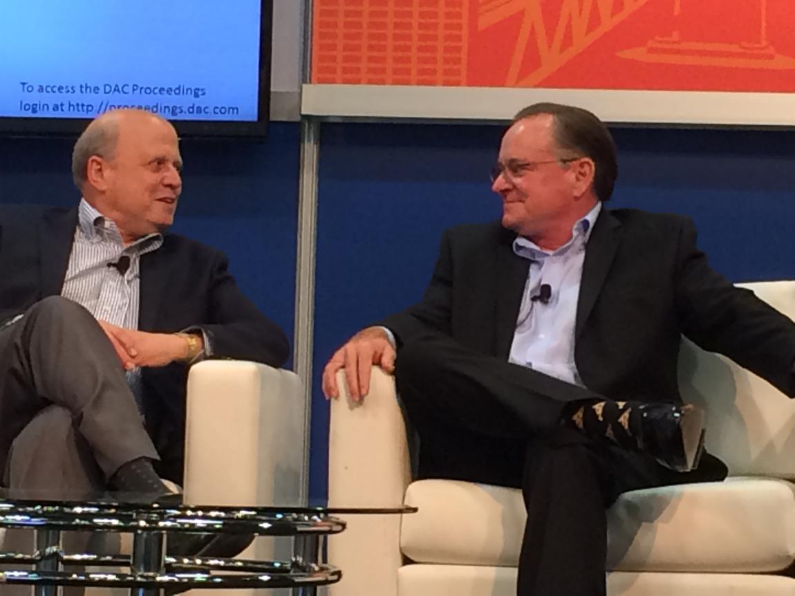
The CEO Fireside Chats were my very favorite part of #52DAC. Dr. Walden Rhines, Lip-Bu Tan, and Dr. Aart de Geus are heroes of the EDA industry, absolutely. I saw all three Fireside Chats and the one word that I’m left with is INSPIRED!

Paul McLellan did a nice write up of the third Fireside chat here:
I Don’t Know Much About Aart…
Paul and I had dinner with Aart the night before so we had the inside track on this one. Richard Goering did a nice write up of the second chat here:
DAC 2015: Lip-Bu Tan, Cadence CEO, Sees Profound Changes in Semiconductors and EDA
And of course I did the first chat with Wally. Unfortunately they were not recorded so I needed to circle back with Wally for this one. In fact, no recordings or pictures were allowed for whatever reason but my beautiful wife was sitting in the front row and could not resist. Those are pizza slices on my socks by the way. My daughter buys me weird socks and laughs when I wear them but I digress…
Why did you choose to attend Stanford and how did you select your major?
Stanford was THE place to go when I started graduate school—great reputation, already known for solid state electronics and fun, fun, fun in the California sun (after four years of miserable weather at the University of Michigan and eight weeks of July heat at Ft. Benning, GA)
What brought you to EDA?
I worked in all aspects of the semiconductor industry but I always found design and product definition to be the most satisfying. When I left TI, I was under a “non-compete” agreement so I couldn’t join a traditional semiconductor company. EDA seemed like the right direction.
How is Mentor doing?
Really well: five years of compound average growth in revenue of 9% and operating profit growth of 30%. More importantly, we’ve been able to ride some waves of change that have been really exciting, particularly the rapid growth of emulation, the emergence of the automotive industry as a major EDA and embedded software user, and the rapid advances in design for test.
What does the future hold for the fabless semiconductor suppliers?
It looks very bright. Historically, TSMC has made most of the profit but competition is becoming more intense while demand grows. Advanced nodes are proving to be very profitable and demand is strong across a broad range of technologies, with 90% of capacity filled at the leading edge and 80% at the trailing edge of technology, so it appears that almost all of our foundry partners are making money. In addition, packaging is become a point of greater leverage, helping the growth of the test and assembly providers. For EDA companies, close relationships with all the foundries and contract assemblers is a fundamental requirement.
What is the impact of the recent consolidations on the semiconductor industry?
Apparently there are significant potential economies of scale, given the large synergies these merging companies are promising. If achieved, they should increase semiconductor profitability and grow demand.
Is the industry consolidating?
It certainly has been over the last year or so. But it’s not as substantial as it might appear on the surface. Combined market share of the largest semiconductor producers has increased several percentage points. This isn’t very much when you consider that the combined market share of the top 50 semiconductor companies DECREASED about ten points over the last decade.
What are the big, unsolved challenges in semiconductor design we should be focusing on?
The top of the list continues to be power dissipation; FinFET has dramatically impacted leakage-related power but dynamic power is still a big issue. Next is functional complexity; most of the “big digital” designs of the industry are moving, or have moved, to emulation as a mandatory complement to simulation. In addition, there is an emerging list of new design issues because of semiconductor physics at leading edge feature sizes—reliability, electromigration, signal integrity, systematic yield problems, patterning and many, many more.
How does the transition to 10nm compare to the transition to 16nm/14nm?
The good news is that the transistor structure remains similar to 16/14nm. The bad news is that, because we don’t yet have cost effective EUV production, the processes have become more complex, involving self-aligned double patterning or triple patterning. Much of this complexity is shielded from the designer by the EDA tools but some of the process complexity requires new design techniques. An example is the effect of coloring: differences in the parasitics for two different colors on the same layer will require some creativity on the part of designers.
What are some of the physical design challenges for FinFET?
Two that come to mind are increasingly complex parasitic effects and testability. Parasitic analysis with FinFET’s is requiring the accuracy of a 3D solver that operates with the performance of a classic 2D one. For test, the variation in fin characteristics of the FinFET means that most designs will adopt cell-aware design for test technology so that they can comprehend transistor level defects that have traditionally been ignored.
Why the renewed interest in analog design at Mentor with the acquisition of Berkeley and Tanner?
Analog and mixed signal technologies have always been important at Mentor; we just lost the lead along the way. Berkeley Design Automation offers substantial performance differentiation, compatibility with existing flows and lots of new capabilities. It’s growing rapidly and brings Mentor into head-to-head competition on the toughest analog and mixed signal designs. Tanner brings us to center stage for the Internet of Things, offering low cost front-to-back design approaches for the hundreds of companies designing low to medium complexity chips dominated by analog and power considerations, or requiring MEMS or photonic capability. Overall, growth in the number of analog and mixed signal designs will be much faster than traditional digital designs.
What does ‘Shift Left’ mean to you?
It means finding problems earlier in the design process when they are much less costly to fix and when there are more degrees of freedom to fix them. “Big digital” designs today verify all of the functionality and much of the embedded software on the emulator, release the design and then verify the rest of the application software on the first prototypes or on FPGA cards. Progress in high level design is gradually moving the design and power/performance tradeoffs to the pre-RTL stage.
What will fuel the demand for emulation going forward?
The industry is in one of its major transitions. Each new design becomes more complex than the last one and, at some stage, simulation alone becomes inadequate. The share of digital designs using emulation will continue to increase every year for a long time.
What is driving the increase in electronic complexity in today’s vehicles?
Instrumentation, driver assistance features, in-vehicle infotainment, networking, safety, security, fuel economy, and more. Electronics have become more than a third of vehicle cost and provide much of the differentiation.
Why is Mentor focused on automotive and aerospace?
It’s not a new endeavor for Mentor. Our first automotive-specific EDA tools were introduced in 1991, focusing on design of wiring harnesses. That family of products grew to become an enterprise-wide set of capabilities from product definition through vehicle maintenance. Today, embedded software offerings for automotive applications are just as big a business for us, with special capabilities for electronic vehicle architecture, audio and video. Altogether, transportation (automotive and aerospace) revenue is approaching 20% of Mentor’s total revenue.
What’s needed to create the billions of devices at the edge?
There will be tens of thousands of different designs that integrate analog, digital, sensor, MEMS, imaging or other technologies. The big challenges will be packaging, integration of disparate technologies, ultra-low power, communication, and reliability. It’s a different vector from traditional digital design. Many of these applications require very low cost, easy to master tools; that’s one reason why Tanner EDA makes sense for us in a growing IoT world.
What’s needed on the digital side?
Big data means “big digital”. Networking and data processing chips will increase in complexity to challenge the limits of verification technology, embedded software, physical implementation, yield analysis and manufacturing. New approaches like silicon photonics are being developed to handle massive data while consuming much less power.This is where the EDA industry shines, meeting the challenge of these problems with new types of verification approaches and design tools.


Comments
There are no comments yet.
You must register or log in to view/post comments.