
I have often written in Semiwiki about high speed PHY IP supporting Interface protocols (see for example this blog), the SoC cornerstone, almost as crucial as CPU, GPU or SDRAM Memory Controller. When you architect a SoC, you first select CPU(s) and/or GPU(s) to support the system basic functionality (Processor for Mobile application, Networking, Set-Top-Box etc.), then you define the various protocols to be supported by this SoC to interface with the functional system and the outside world. For an enterprise system, you will have to select one or several protocols among Ethernet (10G KR & KR4, 40G or 100G), PCI Express 3.0/2.1/1.1, SATA 6G/3G/1.5G or OIF CEI-6G and CEI-11G, to name a few. If you have read this previous blog (or if you have been exposed to high speed PHY utilization), you know that a 12 Gbps PHY IP design is complex, resource intensive and time consuming, as it may sometimes require several Silicon Test Chip before being 100% functional.

Chip makers have to face another challenge. As the cost of IC design rapidly increases due to the reduction in feature sizes, companies are no longer designing products that target just a single application. The SoC design must be architected to utilize multi-protocol physical layer (PHY) IP which can be connected to multiple different protocol controllers/MACs. Here comes the multi-protocol PHY concept. We may have to take a look at the picture below before going further:
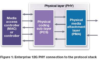
The Physical layer is made of two sub-functions, the Physical Media Attachment (PMA), essentially analog and hard-wired, and the Physical Coding Sub-layer (PCS), digital and soft coded. If you architecture the physical layer in such a way that the PMA can be common to various (say N) interface protocols, and mux N protocol specific PCS, you can optimize analog design resources and cost, and certainly accelerate schedule when comparing with the design of N completely different PHY (except if you have an infinite source of analog designers, but does it really happen in any company)?
We can see the benefit in term of cost and schedule for the PHY IP vendor, but does it also imply a benefit for the chip maker, IP vendor’s customer? When this chip maker is targeting multiple applications, and need to optimize cost, designing only one SoC (or one SoC platform) which can be configured to address these various segments, integrating a single, multi-protocol PHY will certainly improve this IP “cost of ownership”. The PHY integration into the SoC workload will be minimized (one PHY IP instead of N PHY IP). The PHY qualification, using expensive lab hardware, and probably validation boards, will be simplified. Nevertheless, the two most important benefit will be NRE expenses improvement (divided by N in theory), and even more important, better time-To-Market (TTM). In fact, the chip maker benefit from the same TTM improvement than the PHY IP vendor! In the real world, designing and validating a multi-protocol PHY IP takes probably longer than for a single protocol… but the diversity of protocols is such that no IP vendor could bring to the market these N protocol specific PHY as quickly as this multi-protocol PHY.
Does a multi-protocol PHY IP improve TTM for Enterprise SoC chip makers? Certainly yes…providing that this PHY IP supports the protocols you need for your SoC interfaces. Let’s take a look at the protocol list supported by Synopsys’ 12G PHY:
- IEEE 802.3 10G and 40G backplane (XAUI, KR & KR4), port side 40G, 100G (CR4 & CR10), and 10G (XFI, SFF-8431/SFI)
- IEEE 802.3az Electrical Energy Efficient
- SGMII, and QSGMII
- PCI-SIG PCI Express (PCIe) 3.0/2.1/1.1
- SATA 6G/3G/1.5G (Rev 3.2)
- OIF CEI-6G and CEI-11G
- CPRI, OBSAI, JESD204B
This multi-protocol PHY targets the SoC Enterprise market, and most of the relevant protocols are supported. We have not mentioned the PHY specific, complexes features, up-to-date PHY design techniques, like CTLE and DFE, PRBS or in-situ testing:
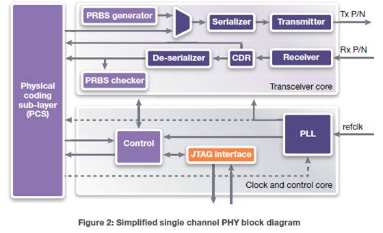
- Multi-featured (CTLE and DFE) receiver and transmitter equalization: adaptive equalizers have many different settings, and in order to select the right one there needs to be some measure of how well a particular equalization setting works. The result will be to improve Rx jitter tolerance, ease board layout design, and improve immunity to interferences.
- Mapping the signal eye and output the signal statistics via the shown JTAG interface: this allows for simple inspection of the actual signal. This in-situ testing method can replace very expensive test equipment (when a simple idea gives the best results!)
- The pseudo-random bit sequencer (PRBS) generator send patterns to verify the transmit serializer, output driver, and receiver circuitry through internal and external loopbacks (keep in mind that Wafer level Test equipment are limited in frequency range, such a circuitry allows running test at functional speed on a standard testers).
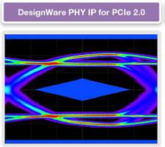
If you are interested by Eye diagram measurement, and more specifically want to know how to reduce PCI Express 3 “fuzz” with multi-tap filters, you definitely should read this blog from Navraj Nandra (Marketing Director PHY & Analog IP with Synopsys). The very didactical article explains how adaptive equalization works, Inter Symbol Interferences (ISI), as well as help to understand how signals contain different frequency content, illustrated by four examples of forty bit data patterns. Navraj has been able to explain advanced signal processing concepts by using simple words, and this is everything but simple to do!
From Eric Esteve from IPNEST
More Articles by Eric Esteve…..
lang: en_US
Share this post via:


Comments
There are no comments yet.
You must register or log in to view/post comments.