
If we check the many articles daily published in Semiwiki, I am sure that Moore’s Law has been mentioned every single day. There is a good reason why we constantly write about new technologies and advanced features like FinFet, FD-SOI, 450 mm wafers or double patterning: all of these are new challenges that the SC industry will have to take up. As designs migrate to smaller process nodes, such as 20-nm and 16-nm FinFET, the technology challenges to extend Moore’s Law become increasingly complex. TSMC has implemented double patterning mask technology on its 20SoC process utilizing two photo masks, each with half of a pattern, to enable printing of images below the node’s minimum spacing design rules. We know in 2013 that the most wonderful technology would be useless if it’s not supported by IP vendors, developing the “LEGO” blocks you need to successfully design a SoC. Those who read my articles know how crucial it is for the SC industry to benefit from high quality PHY IP, allowing supporting High Speed Serial Interfaces protocols, like USB, DDR, PCI Express®, and MIPI®.

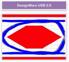
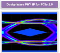
The above picture is obtained from Synopsys TSMC 20 nm Test Chip characterization of the PHY (here an USB 2.0 PHY), and is representative of the quality of the design. We call it an EYE diagram: if the signal generated by the PHY is well built by the on-chip circuitry, then this EYE will be well open, so you can insert this red form within it and that’s the guarantee that the Interface will work as specified (at 480 Mbps in this case). Porting an existing PHY design, validated on an older technology node (larger gate length and different design rules) is absolutely not straightforward; it may happen that a complete redesign could be a shorther path. Synopsys’ development of DesignWare IP and Interface PHY at 20-nm focused on minimizing yield and manufacturability issues while adhering to the standards’ specifications, as well as TSMC’s advanced layout and design rules for manufacturability with double patterning technology. The result of these efforts can be seen on this EYE diagram for the PCIe 2.0 PHY IP:
A very interesting point is made by John Koeter: “As the leading provider of physical IP with more than 80 test chip tape-outs in 20- and 28-nm, Synopsys is focused on developing IP in the most advanced process nodes to help designers take full advantage of the processes speed and power characteristics while implementing high-quality, proven IP,” said John Koeter, vice president of marketing for IP and systems at Synopsys. “By offering a broad portfolio of IP for the 20-nm process, Synopsys enables designers to more easily meet their goals of creating differentiated products with less risk and faster time to volume production, while also reducing the risks associated with moving to the 16-nm FinFET process.”
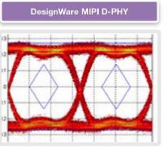
What type of application will be targeted by SoC designed in TSMC 20 nm, and later 16-nm FinFET processes? Most probably mobile, smartphone or media tablet, for three main reasons: chip cost (area), performance and power consumption. Synopsys is claiming that TSMC’s 20SoC process enables designers to reduce the power consumption by up to 25 percent or increase performance by 30 percent. Mobile application are known to be MIPI friendly, that’s why the last EYE diagram is for MIPI D-PHY:
Availability
The Synopsys DesignWare USB 2.0 PHY, USB 3.0 PHY, DDR4 multiPHY, PCI Express 2.0 PHY, and MIPI D-PHY for the TSMC 20SoC process are available now, just click to get more information about silicon-proven Synopsys DesignWare USB, DDR, PCI Express and MIPI PHY IP.
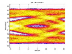
If you want to take a look at an EYE diagram being Analog designer’s nightmare, this one is a good example:
Eric Esteve from IPNEST
lang: en_US


Comments
There are no comments yet.
You must register or log in to view/post comments.