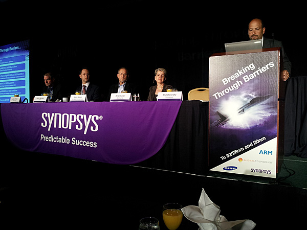
Tuesday morning at DAC I attended the Synopsys-hosted breakfast to hear from foundries and ARM about the challenges of designing and delivering silicon at the 32nm/28nm and 20nm nodes.

Phil Dworsky (Synopsys)
Drivers in the industry: SW, social media, cloud infrastructure, mobile convergence, Internet of things.
Smart electronics – how to keep the battery life going?
Cloud infrastructure – maximum performance desired.
Smart device – max performance, long battery life, cheaper than before.
Barriers – gigascale complexity, pressure for turn around time, double patterning, 3D IC.
Collaboration between foundry, design and EDA is mandatory now at 28nm and 20nm.
QR codes are being used for a Synopsys contest, scan more and get points to win prizes.
Ana Hunter, Samsung
Foundry – partnership started in 2005 with IBM, ST, GLOBALFOUNDRIES. Proven IP with ARM and Synopsys. Supply of wafers, safety with Common Platform Alliance.
Technology – low power for mobile is a focus. 20nm and 14nm now in development, gate last for 20nm and FinFET for 14nm well underway in the labs.
PHysical IP – ARM, processor cores – ARM.
High speed interfaces – Synopsys.
Samsung and other IP partners round out the IP offerings.
Packaging for mobile – System in package, package on package using laser drilling, TSV is in development (requires collaboration with Synopsys tools). Memory design at Samsung helps out customers that need memory integration.
Assurance of supply – Samsung spending $7.7B for logic fabs this year, expanding Korea and Austin fabs.
Design enablement – Library/IP, PDK, DFM, Design Technology.
Design Technology co-optimization – how to get most out of cells and tools together.
PHysical IP – a 6 year relationship so far using Logic LIbraries, Memory Compilers, Programmable Options and Interfaces (DDR3).
Design Tools – qualification last year of 28nm process along with Galaxy tools, silicon verified.
45nm to 32m transition – power consumption reductions of 48% on GPU and 45% on CPU. This should put to rest the FUD on our technology.
20nm is tougher because it requires DPT and rule explosion (2.5X more rules for metal routing alone). IP must be compliant with DPT, so ARM and Synospys are inline to deliver.
Early 20nm test chip is a a Design TV Implementation – Memory, cel library, ARM Cortex Macro, IO pads, interconnects, oscillators, etc.
Conclusions – 32nm HKMG gate first ARM SOCs are in volume productions. At end of 2012 the majority of Samsung fab will run 32nm designs.
20nm is coming, the challenges are being addressed.
Kevin Meyer – GLOBALFOUNDRIES
Focus – getting 28nm into volume production.
Challenge – how to get design drivers like mobility into new process nodes.
Looking back to 2009 – Artisan acquired by ARM, Synopsys tools, Synopsys IP. Enable fabless and fab-lite companies, vertically optimize the design process.
In 2011 continued emphasis on using ARM cores as drivers in new SOCs.
GLOBALFOUNDRIES has a history of high performance process design from AMD. Reached 2.5GHz speeds on ARM cores for performance and 2.0GHz on low power processes.
20nm – already taped out using an ARM Cortex core and in fab now.
HKMG shipments in highest volume now compared to any other foundry. Yields at .1 Bose-Einstein constant. 400K wafers shipped to date with HKMG now, it’s working.
Foundry capacity: Germany, Singapore, New York.
In 4Q11 became the #2 foundry, passing up UMC. Growth seen in Smartphones and Tablets using low power processes.
High performance computing – 28HPP
Mobile – 28SLP, 28LPH
Wired – 28HPP
2013 – expect 20nm process called 20LPM, also 20LPW.
2014 – expect 14nm FinFET processes.
28nm challenges – use the same HKMG stack from 32 nm (proven). 100% density improvement, 40% faster, 40% less power.
20nm – full shrink from 28nm, 100% density increase, 40% performance increase.
POP – Processor Optiization Pack work continues in 2012.
Collaboration – includes adding other IP and EDA vendors, assembly, masks, assembly, test.
Dr. John Heinlein – ARM
Markets – Tablets, Superphone, mass market smartphones, entry level smartphones.
Cores – Cortex A8 from 2009 up to Cortex A15 in 2012. New Big/Little core architecture continues to grow, both high performance and low power by working in tandem.
At 32nm the collaboration started in 2008 with alpha and beta PDKs, taking about 3 years to production.
For 28nm a validated library was completed in 2012.
At 20nm a validated library program started years ago, and fully validated libraries expected in 2013.
Memory compilers – come and see what we’ve done at 28nm libraries.
Processor Optimization Pack – Artisan IP targeted and optimized for one process node, implemented by ARM and documented for performance, user guide on how to achieve the same results (implementation specific to EDA vendor tools). Create multiple power-performance points based on trade-offs that you can decide. POP gets you a faster time to market.
A Cortex A9 can reach .75GHz up to 1.6 GHz based on trade-offs.
Memory compilers – now targeted at low power using multi VT, level shifters, dynamic EMA, write assist, flexible banking. A new cockpit called MemExplorer helps you choose which RAM instances to achieve your design goals.
John Chilton – Synopsys
2006 the collaboration started with this group using 65nm nodes.
Recent press release between Samsung and Synopsys on a 20nm tapeout.
About 400 tape outs at 28nm.
Best practices for Manufacturing, PDK, Early IP, Production IP, Design Methodology, Calibration and Design Manual (pre-eval, eval, alpha, beta).
32nm and 28nm is completely verified now. Lynx embodies these best practices into a flow and cockpit, including 3rd party tools. Foundry ready kit has PDK, ARM libraries, notes, methodologies, tape out checks, etc. It’s not just point tools, rather a methodology. Using Lynx get to your final performance goals sooner.
A quad Cortex A9 example shown in Lynx cockpit allowing 1st Silicon Success.
Synopsys offers interface IP: USB, DDR, SATA, HDMI, XAUI, PCI Express.
Faster yield ramp with EDA tool called Yield Explorer, spanning manufacturing to design. Helps you identify yield issues, can guide the SEM to pinpoint a small via, etc.
20nm is quite a bit different than 28nm: DPT (increased mask costs, tool complexity), FinFET. Doing litho simulations, early PDKs, first test chips in fab, working towards production IP. Every physical EDA tool has to be DPT aware and upgraded. 25 real designs in development using DPT.
3D IC requires EDA tool upgrades: Sentaurus (Interconnect), StarRC Ultra (Extraction), etc.
Summary
Foundries, EDA and Semi IP design are working closely together to deliver process, tool flows and IP that will work at 28nm and 20nm nodes. The design costs at 20nm will be higher than 28nm for the same gate count, so you need to make an economic decision on what a 20nm design will buy you (more gates, less area, slightly better speed, slightly better power).
Samsung continues to rise in the foundry business and in a few years may replace Intel as the number one semiconductor company in the world as measured in revenue.
Foundries like to differentiate from each other (even when using identical processing) so one way is to offer specialty IP not found anywhere else, which makes opportunities for IP companies to sell into the Foundries.
The big foundries tend to work with the big EDA companies in qualifying tool flows, so make sure that your favorite EDA tool has been qualified at the foundry (unless you like to be the first customer to try out a new tool on a new node).
Share this post via:


Chemical Origins of Environmental Modifications to MOR Lithographic Chemistry