IC reliability is an issue that circuit design engineers and reliability engineers are concerned about, because physical effects like high Current Density (CD) in interconnect layers, or high point-to-point (P2P) resistance on device interconnect can impact reliability, timing or Electrostatic Discharge (ESD) robustness. Common approaches for these calculations include device-based or cell-based checks, and now there are coordinate-based checks to consider using.
ESD Verification
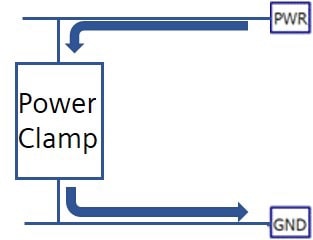
During ESD verification both P2P and CD checking are used to determine if each ESD discharge path is reliable. In the figure below the ESD paths are shown along the gold-color lines, starting at an input pad, passing through power-clamping devices, then ending up a power or ground pad. The design goal is to keep the surge current away from the devices in blue.
To mitigate ESD failures, a layout designer keeps the resistance along the ESD discharge paths low.

Device-based Checks
An EDA tool like Calibre PERC from Siemens EDA can run a device-based P2P check on ESD paths in three steps:
- Extract a layout netlist
- Traverse and find ESD devices, power clamping devices
- Extract and simulate resistance network, measure ESD effectiveness
Your foundry would supply a Calibre PERC rule deck for this ESD analysis to be run, but it’s possible that the PERC rule decks don’t cover all EDS devices or paths. Your company may want to develop custom PERC rule decks for unique ESD structures being used. There’s a learning curve to becoming proficient at writing Calibre PERC rule decks, so creating and verifying custom rule decks will cost you both time and engineering talent.
Cell-based Checks
With cell-based checks you are not considering the details of ESD devices and circuits, rather just the cell names and port names will specify your ESD cells. The upside of using a cell-based check is that run times are much quicker, as the device extraction is disabled during the LVS layout extraction step. This second figure shows the cell-based verification approach:

Your Calibre PERC rule deck still has cell names and pins defined, however the downside is that the accuracy of results will be less than that of device-based checks.
Coordinate-based Checks
A design or layout engineer will want to calculate P2P resistance between two coordinate points of a net in the IC layout, before the full-chip verification has been run. When a new IP cell is adding to a chip layout, the team needs to know that power and ground connections are solid. There may also be special nets that require identical lengths between cells.
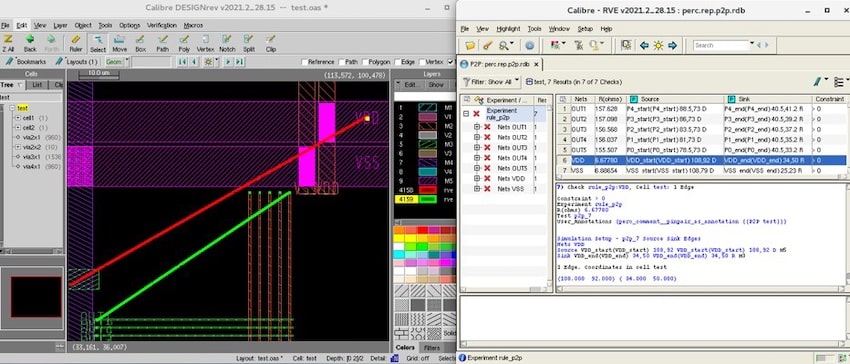
With coordinate-based checks for layout verification, there is no requirement to write a Calibre PERC rule deck defining devices or cells, so it’s a quicker and easier method to run than P2P and Current Density checks. You do need to define some coordinates for start and end location along a net, along with a layer name, also called probe points. LVS device extraction can be skipped in coordinate-based checks, producing P2P and CD results quickly.
Your probe mapping file is a simple ASCII format, easy to create from a cell’s text file, and the cell coordinates in the top cell. Results from a coordinate-based P2P check are shown next:

Summary
There are three possible methods for P2P and current density checks when using the Calibre PERC tool:
- Device-based: most accurate, requires rule deck knowledge, slowest run times
- Cell-based: less-complex rule decks, fast run times
- Coordinate-based: no changes to rule deck, fast run times
Familiarity with the rule deck language is required when using the device-based method, and with advanced nodes an ESD MOS device can have thousands of fingers, slowing down the P2P and Current Density calculations.
The second method introduced, cell-based checks is quick to start using, has an easier rule deck, and enjoys faster run times than device-based checks. So you can always trade off speed and accuracy of results.
The final method of coordinate-based checks has minimal rule deck changes to get started, and the results are easy to debug with RVE, ideal to use for quick layout check when in the initial stage of designing and verifying an SoC.
Read the full nine page White Paper from Siemens EDA here.
Related Blogs
- AMS IC Designers need Full Tool Flows
- Symmetry Requirements Becoming More Important and Challenging
- EDA in the Cloud – Now More Than Ever
- RealTime Digital DRC Can Save Time Close to Tapeout
- Transistor-Level Static Checking for Better Performance and Reliability


Comments
2 Replies to “Methods for Current Density and Point-to-point Resistance Calculations”
You must register or log in to view/post comments.