If you don’t get the tongue in cheek reference of the title, you probably don’t have children who liked to watch Disney movies. All four of my daughters loved Disney and so, I am forever shaped by the Wonderful World of Disney. In 2007 Disney adapted to the screen a novel called, ‘A Bridge to Terabithia’, in which two adolescents escape (at least temporarily) into a make believe world of wonder and magic. Sometimes when I read about all of the work going on in electrical-optical (E-O) design I get the feeling I’ve been dropped into such a magical world.
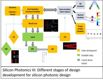 In one of my previous articles, “TheGuiding Light and Other Photonic Soaps”, I brought out the dichotomies between electronic and photonic design and exhorted all to us to think hard about the need for building bridges between electronic and photonic design automation tools, later referenced as EPDA tools. It seems that some of these bridges have already been built and that there has been much progress towards putting together viable E-O design flows. Friends in the EPDA world provided me with existential proof of the work that is pulling these two very diverse industries together. Examples cited included a host of papers about silicon photonic design rule checking, equation based DRC verification methodologies, scalable photonic design environments using PDKs, LVS checking for photonic ICsand even two books that talk extensively about design flows for E-O type designs (Silicon Photonics IIIand Silicon Photonics Design: From Devices to Silicon).
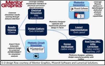
They also pointed to E-O bridges that have been built between Mentor’s Pyxiscustom design tools and Calibre ICverification tools with photonic tools from Lumerical Solutionsand PhoeniX Software. In this cited flow Mentor’s tools are responsible for the electronics portion of the design while Lumerical’s circuit simulator, INTERCONNECT, is used to simulate the optical portions of the design and PhoeniX Software’s OptoDesignersoftware is used to do photonic waveguide routing. All of these tools are working in a fairly integrated environment allowing designers to share information back and forth between the electrical and optical domains. A similar flow has also been put together between Mentor’s Tannercustom design tools and Luceda Photonics’ IPKISStool. I’m told that all of these tools have been deployed at several customer sites and are now being put to the test on real E-O designs looking to operate in the Terabyte-per-second regime. Thus the tongue-in-cheek reference to Terabitsia, except in this case it’s not magic. It’s real!
 On a related but different front, there are also a growing number of photonic training sessions being given around the world to bring more electronic and photonic designers up to speed on these new E-O flows. Examples of this include an edX course entitled, ‘Silicon Photonic Design, Fabrication and Data Analysis’ hosted by Professor Lukas Chrostowski of the University of British Columbia. In Professor Chrostowski’s course students used a cloud-based training environment that used the Mentor Pyxis and Lumerical INTERCONNECT tools to learn how to design, fabricate and test photonic circuits. Student designs were fabricated and tested and results were sent back to the students for them to analyze how their design really worked after manufacturing. In his next edX course, Professor Chrostowski will be showing new methodology developments and his approach to simulating on-chip device and waveguide variation. This is becoming more important as photonic IC designs scale in complexity.
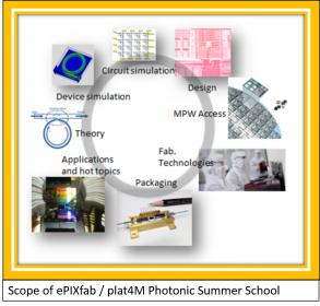 Similarly, an industry group known as plat4Mis collaborating with the Europe Silicon Photonics Alliance (ePIXfab) and several EPDA vendors to host a Silicon Photonics Summer School in August of this year at Ghent University, in Belgium. This hands on session will use the Mentor Tanner and Luceda tools to train participants in silicon photonic design, circuit level simulations and design-rule compliant layout using PDK-based design methodologies.
Lastly, no bridge is useful without a firm foundation and in this case that foundation comes in the form of electronic and photonic process design kits (PDKs). Plat4M, a European funded project to enable a seamless transition of silicon photonics research platforms to industry and ePIXfab, an open alliance of European organizations who mission is to promote silicon photonics science and application, have been instrumental in working with EPDA vendors such as Mentor Graphics, PhoeniX Software and Luceda towards the offering of well-characterized photonic PDKs that can be used in these new E-O based design flows. This has been echoed by PDK offerings from a multitude of photonic foundries such as imec,CEA-Leti,ihp,VTT,SmartPhotonics,Fraunhofer HHI,LioniX,Oclaro,IMEand now Sandia National Labsand theAIM Photonicsinitiative in the United States.
While E-O designs are not wide-spread yet, interest in their application is growing and becoming more important in areas such as Telecom, Datacom, Space and Defense, Sensors, Security, Transport, Energy and Environment to name just a few. Perhaps the bridges being built are indeed leading us to Terabyte-per-second speeds and a whole new world that will indeed seem like magic!


Comments
There are no comments yet.
You must register or log in to view/post comments.