The prevailing industry trends are clear: (1) PCB and die package designs are becoming more complex, across both mobile and high-performance applications; (2) communication interface performance between chips (and their related protocols) is increasingly demanding to verify; (3) signal integrity and power integrity issues are more intricate (e.g., the impact of power distribution noise on nearby signal integrity); and significantly, (4) the design resources with detailed SI and PI expertise are very limited. Project schedules are often adversely impacted by both the available bandwidth of the SI/PI specialists and the long iterative loop between board design, model extraction, SI simulation, and feedback to the physical designers.
The industry requires an integrated design environment, where SI/PI analysis can be launched easily, run quickly, and provide accurate results back to the designer. Although perhaps obvious, the same fast/accurate requirement applies to design rule checking for manufacturability and EMI/EMC compliance.

I recently had the opportunity to speak with Dave Wiens, Business Development Manager, and Dave Kohlmeier, HyperLynx Product Line Director, at Mentor Graphics, on how the HyperLynx development team is addressing these challenges. Indeed, they were excited to convey features in the latest HyperLynx release that offers a significant productivity boost to designers. Here are some of the highlights of our discussion.
Performance
Signal integrity verification consists of setup, simulation runtime, and post-results analysis. Setup involves generation of models (e.g., S-parameters for non-uniform 3D regions) for SI simulation, and is often a time-consuming step.
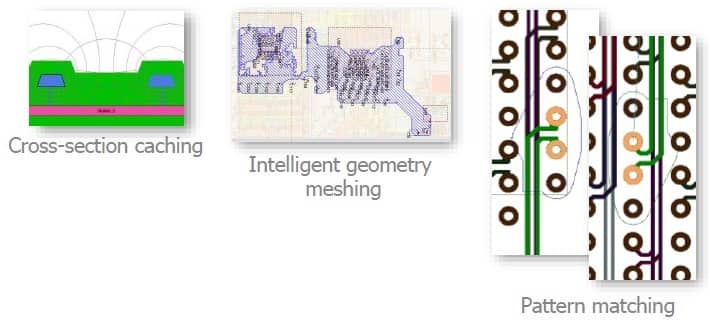
For this release, the HyperLynx team incorporated unique features to accelerate tool performance — i.e., advanced pattern matching, and cross-section caching — as depicted in the figure below:

The result is that (thousands of) cached structures enable extensive reuse during model build. Performance is further improved through multi-threaded execution.
And, a key feature is the automatic definition of sections of the design model to be directed to specific integrated solvers — e.g., structures that require 3D full-wave analysis are identified and detailed models generated. The judicious application of 2.5D and 3D engines to their respective geometries improves setup performance dramatically.
The tool environment also includes the familiar HyperLynx design wizards. In Dave K.’s words, “The wizards embed domain knowledge to conduct a small interview with the designer to identify model details for analysis, such as the DDRx Wizards. These applications provide both an easy-to-understand design reference, and an overall boost to post-results analysis productivity.”
Accuracy
Performance improvements would be of little value, if model simulation accuracy is compromised.
As mentioned above, 3D full wave field solver methods are applied to appropriate structures, such as differential vias. The ports introduced by this model partitioning are managed automatically, when re-constructing the full model. Full-wave solvers utilize excitation sources and reference planes to analyze the structure, for calculation of EM fields. As these sources/planes do not represent the exact field profile at the ports, there is a source of error. Calibration “de-embedding” of port discontinuity errors from this partitioning is crucial to model accuracy, and is also automatic.
Resulting Touchstone S-parameter files — with potentially very many ports — are analyzed for quality (e.g., passivity, causality, reciprocity). The Touchstone Viewer also provide visual feedback of model characteristics, such as insertion loss deviation, return loss, insertion loss to crosstalk ratio, etc.
Algorithmic support is included for the most advanced trace surface roughness and frequency-dependent dielectric models.
Optimum geometrical meshing of the structures also ensures the appropriate accuracy/runtime tradeoff.
HyperLynx supports the recent power-aware IBIS model standard, to accurately reflect the impact on signal integrity due to coupling through the power distribution network (PDN) — e.g., simultaneous switching noise on a parallel interface, and via-to-via coupling through the PDN.
HyperLynx performance and accuracy are industry-leading for analysis of DC drop in the PDN, and calculation of the PDN frequency-dependent impedance.

In addition, the latest Hyperlynx release environment includes a new capability for advanced SerDes signal integrity analysis.
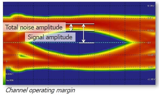
An emerging approach to validation of channel performance is the Channel Operating Margin, or COM, calculation. (This is the de facto analysis methodology for the 100 Gigabit Ethernet standard.) For SerDes protocols that support the COM method, such as 100GbE, simulation support is provided in HyperLynx to generate the channel pass/fail margin result.
Mentor has been a leading proponent on the definition of COM measurement techniques — for more information on COM and recent recommendations for improving the accuracy of COM simulation to BER measurement, please refer to the following article.
In addition to the SI/PI features mentioned above, HyperLynx DRC performs PCB full-board design rules checks, detecting both irregular physical topologies and EMI/EMC structures of concern, such as interrupted signal return paths.
Usability
HyperLynx is an integrated suite of analysis applications, available in a single user environment, with a unified data model.
Both Dave K. and Dave W. emphasized that the HyperLynx team has focused on usability (and a quick learning ramp), while not compromising accuracy. The theme of our discussion was “the fastest time to accurate results”.
I think these guys are on to something. From an overall project perspective, the SI/PI specialists in the organization are inevitably stretched thin, often supporting multiple board and package designs. An integrated environment for physical designers, with performance optimizations to speed closure while maintaining highest accuracy, is definitely needed.
For more general information on HyperLynx, please follow this link.
-chipguy
Share this post via:


Comments
0 Replies to “PCB Design Requires Both Speed and Accuracy of SI/PI Analysis”
You must register or log in to view/post comments.