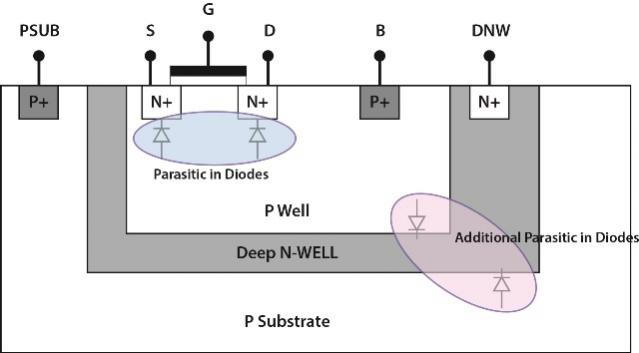
The market demanded that gadgets it loves become ever more conscious of their power consumption, and chip designers responded with an array of clever techniques to cut IC power use. Unsurprisingly, these new techniques added to the complexity of IC verification. When you’re verifying a design that has 100+ separate power domains, plus tightly packed digital and analog parts in the same substrate, proximity effects like noise, latchup, and parasitic effects require more than a basic on-off verification. Because the market also demands that these low-power devices actually work when you turn them on.
 In most cases, traditional LVS methodology is simply not good enough to ensure circuit performance and reliability in these designs, because some design rule checks can’t be performed without adding layout features, and some errors are nearly impossible to debug.
I had a chance to talk to some of Mentor’s engineers who are developing ways to check these new design rules, such as deep n-well biasing, well implant, and extract parasitic effects for mixed-signal SOCs with multiple power domains, using a new approach and new algorithms. Sridhar Srinivasan is the technical lead for Calibre® PERC™, Frank Feng is a methodologist, and Yi-ting Lee is a foundry technical liaison. They presented a paper at the China Semiconductor Technology International Conference (CSTIC) about reliability verification, which you can read for yourself here.
Not surprisingly, power is a hard design problem to generalize. Even the “simplest” device, say, one with four power domains, has thousands of failure points. When you start increasing the number of domains, adding in use cases, varying voltages, etc., and trying to analyze how each power state affects the functionality of other parts that may be turning on or off themselves, it’s pretty easy to understand how power-aware verification gets really difficult really fast.
All three pointed out the need for verification tools that can combine and analyze the netlist and layout simultaneously both to understand power intent and identify a variety of power-related problems. In their work, the trio focuses on several proximity-related issues that can be power-domain-dependent:
- Verifying parasitic junction diodes
- Accuracy of deep n-well biasing voltages
- Identification of devices with latchup risks
- Situations leading to leakage current due to domain crossings
The rule checks that involve these proximity effects combine electrical rule checks and geometry-based DRC rule checks. To solve the verification challenge, they used a netlist-based infrastructure with a programmatic interface to the geometry database that was developed at Mentor Graphics. This technology is available as part of the Calibre® PERC™ product from Mentor Graphics. The inputs to the flow are a schematic netlist, and/or a GDSII/OASIS/LEFDEF layout, and a user-described rule set that includes power, ground, and IO setup. The setup includes the specification of the various power signals present in the system, specification of the known internal supplies, programmatic specification of derived internal supplies based on the circuit structure (like charge pump, level shifter, etc.), and design-dependent property propagation “stop” rules.
First, they said, the tool reads in the netlist representation of the design to construct the graph. Then the user-defined signal specifications are processed—the explicit signal definitions with net names are processed first, followed by the programmatic, structure-dependent specifications. All signal specifications are saved as properties and are propagated through the graph. Srinivasan says they included hierarchical APIs to control the propagation of these properties based on the design device types (PMOS, NMOS, RESISTANCE, etc.), including custom device types, and then let the user specify blocking conditions. After property propagation, the nets in the graph have the propagated data, and the user can then inspect the propagated properties and defined properties through a handy introspection API at each net.
With large and complex designs, runtime is an issue in every step of the flow, including verification. To reduce runtime, the properties can be collapsed. For example, instead of assigning unique properties to each power supply, you can group the power supplies by domains and voltage ranges and assign properties to each group. Srinivasan said that keeping the total number of properties below 64 provides a major performance advantage, as the properties can be encoded without the special data structure needed to create complex bit sets.
The trio performed reliability checks on real-world multiple-power-domain and mixed-signal designs using Calibre PERC in tandem with traditional LVS and DRC…If you’d like to learn more of the details, download the paper (free, but registration required).
As for the next phase? In the future, they said, the Calibre PERC tool will be able to handle device reduction, netlist transformation, and voltage transitions automatically with minimal user input, further improving usability. When it comes to the details, I’m not sure exactly what all that will mean, but I do know it signifies good things for designers struggling with complex power verification at advanced nodes.
Share this post via:


Comments
There are no comments yet.
You must register or log in to view/post comments.