With the advent of large SoCs in semiconductor design space, verification of SoCs has become extremely challenging; no single approach works. And when the size of an SoC can grow to billions of gates, the traditional methods of testability of chips may no longer remain viable considering the needs of large ATPG, memory footprint, and chip pins requirement for DFT and so on. Alternate methods need to be discovered. It pleasantly reminds me that the strategy of ‘Divide and Conquer’ to solve a problem with largeness works well here too. However, it’s easier said than done, in this case one needs to formulate the complete methodology of dividing the design for testability and then also re-combining it to complete the test at the full-chip level. How do we do that?
It’s heartening to see a novel approach developed by Mentor Graphicswhere they use a hierarchical DFT methodology for testing the hierarchical cores and their interconnections separately, step-by-step, leading to full-chip testing.
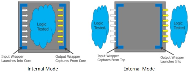
A core is the lowest hierarchical level at which test patterns are applied. It has a wrapper chain that can be configured to test the logic inside the core or the interconnect and glue logic external to the core. The core inside logic is tested in ‘Internal Mode’ when the ‘Input Wrapper’ is configured to launch values into the core and the ‘Output Wrapper’ is configured to capture responses. In the ‘External Mode’, the wrapper chain is reconfigured to launch values from the outputs to test chip-level glue logic and interconnect and capture responses at the inputs. In order to complete the DFT requirements, scan chains, compression logic, and test control logic are also inserted. With that it’s possible to generate a set of scan patterns at the core level that can subsequently be retargeted to the chip level. The end result of this step is a set of retarget-able patterns and a fault list containing all the coverage information for that pattern set. Clearly, the pattern generation time and the memory footprint for complete chip-level testing are significantly reduced by using this approach. Moreover, the procedures for different cores can be parallelised.
During the ‘External Mode’ testing, all of the logic already tested for a core in ‘Internal Mode’ is removed from its netlist (except what is needed for external mode testing) to create what is called ‘graybox netlist’, thus making it possible to test the entire SoC without loading the full-chip netlist. In this process, a netlist reduction and hence memory footprint reduction of 10x or more can be easily possible, although it’s design dependent.
For full-chip testing, retargeting of scan patterns at the full-chip level depends on how the cores are configured to be tested in ‘Internal Mode’ in the overall architecture of the chip. A mapping of ‘Internal Mode’ scan patterns from the core pins up to the chip-level pins has to be done. The pattern sets of multiple cores must be merged such that they can be simultaneously applied at the full-chip level.
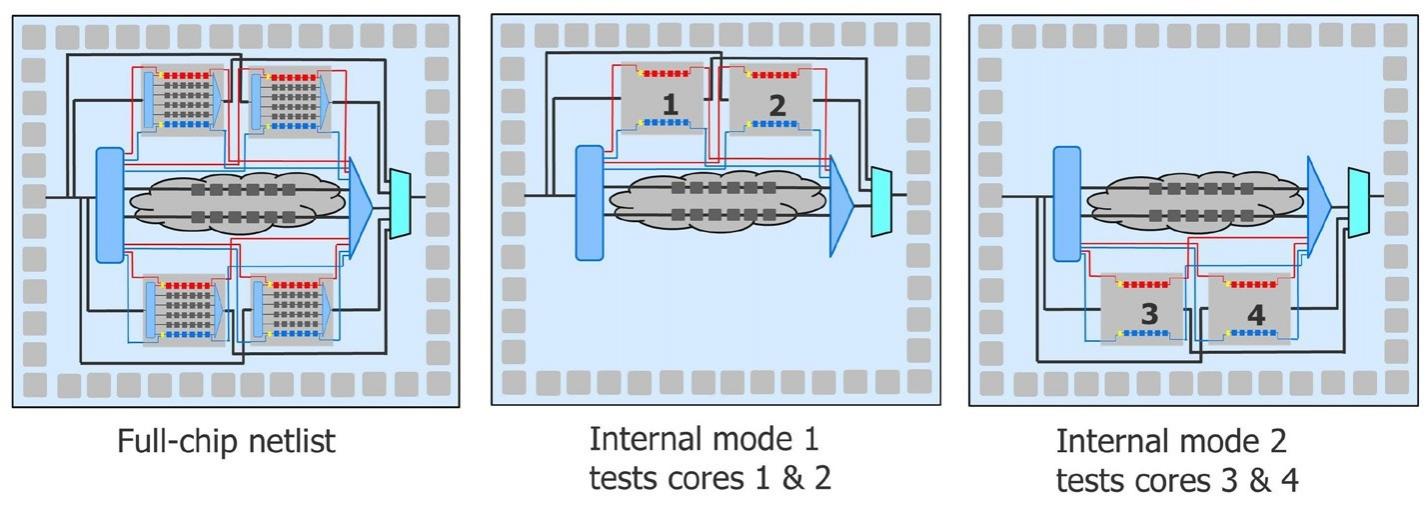
Above example shows how ‘Internal Mode 1’ groups cores 1 and 2 together whose patterns are retargeted and merged together. Similarly in ‘Internal Mode 2’ cores 3 and 4 are grouped together for retargeting and merging their patterns.
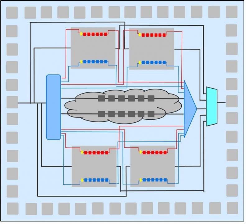
After testing all cores, the interconnect and glue logic between cores is tested in external mode. The chip-level netlist is minimal in content with graybox netlist for each core. The external mode configuration accesses all the wrapper chains of the cores as well as any chip-level scan chains and runs the ATPG. After completing this testing, the final test coverage of the entire chip is computed by merging the fault lists saved from each core’s ‘Internal Mode’ pattern set into the ‘External Mode’ fault list.
The DFT tool automation in Mentor’s Tessent tool suite supports this hierarchical methodology where all procedures as described above are automatically done. In fact, dedicated wrapper cells are not added all the time in order to conserve area and time. Instead, Tessent Scan automatically identifies and stiches shared wrapper cells (i.e. existing functional registers that can also serve to isolate primary inputs/outputs for test purposes) where possible.
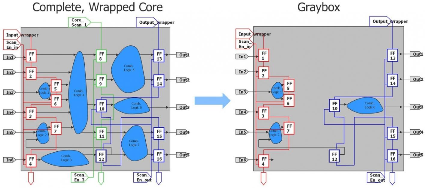
Above is a typical circuit example of a complete wrapped core with complete core netlist and its graybox representation. In the graybox, only wrapper chains and any combinational logic between the wrapper chains and the primary inputs/outputs of the core are required. This can reduce the netlist in the range of 10x to 20x. Tessent TestKompress automatically generates the graybox netlist.
Tessent TestKompress includes all the pattern retargeting functionalities as described above along with the clock control logic and other requirements. Rick Fisette has described all these procedures in great detail in the whitepaperposted at Mentor website.
With some up-front design planning, this methodology provides an excellent solution for the challenging task of testing large SoCs. The additional design effort required in this methodology is compensated richly in terms of at least 5x reduction in ATPG runtime, significant reduction in memory footprint (can be 10x or more depending on design), significantly reduced cumulative time, reduced pressure on tapeout as any ECO may affect a particular core and hence initiate retesting of that core only, and reduced dependence on top-of-the-line machine for testing. It’s simply a great methodology!

More Articles by Pawan Fangaria…..
lang: en_US
Share this post via:


Comments
0 Replies to “Taming The Challenges of SoC Testability”
You must register or log in to view/post comments.