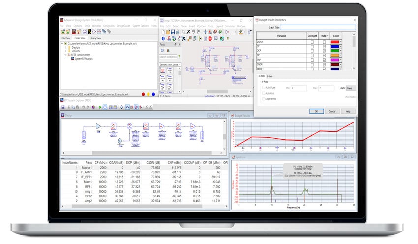
Video webinars are a main staple to learn what’s new about EDA tools and methodologies, but there’s nothing quite like meeting in person, where you can ask questions and gauge the expertise of the presenters. I was delighted to learn that Keysight is planning a literal world tour to update EDA customers and prospects on what they have to offer for IC groups doing high-speed, high-frequency and high-power designs. Technical experts from Keysight will be visiting over 20 cities starting January 16th in Paris, then finishing in Boston by May 16th, and there will even be customer presentations that vary by each region.
At the Keysight EDA Connect World Tour, you will hear about the exciting innovations and challenges in four industry mega-trends:
- 5G/6G – Topics include how to meet the demand for higher accuracy, sensitivity, and bandwidth for 5G NR, and how to keep up with emerging new standards with 5G NTN (Non-Terrestrial Networks), 6G networks, and security.
- Aerospace & Defense – Learn about the latest developments in satellite communications and how to manage interference for electronic warfare and radar systems.
- Semiconductor – Amid supply chain disruptions and engineering shortage, the sessions will explore opportunities in new materials, silicon photonics, 3D IC, and co-packaged optics.
- Consumer & Automotive – The sessions will cover new memory and interface standards like DDR5, PCIe 5.0, and HBM4. design for high-power, chiplets, miniaturization.
No matter your role in the IC world — from design engineer to R&D team leader — this World Tour has something valuable for you. The technical presentations focus on four key areas:
- RF circuit designers working on MMICs for applications such as 5G/6G, automotive radars, Wi-Fi, and WiGig.
- Digital designers who design and simulate the layout and performance of PCBs.
- RF system designers creating RF transceiver systems in commercial wireless, A&D, and radar applications.
- Device modeling engineers creating robust RF and GaN device models.

Some of the presentation topics include AI-driven design, chiplets, and 3D integration plus live product demonstrations of the newest features in the Keysight EDA tools. Locations and dates are listed below:
- US: San Diego – Feb 7, Santa Clara – Feb 28-29, Austin – Apr 10, Dallas – Apr 11, Denver, Apr 25, Colorado Springs – Apr 24, Boston – May 6
- Europe: Kista – invite only, Paris – Jan 16, Nijmegen – Jan 18, Toulouse – Jan 22, Catania – invite only, Rome – Jan 24
- Asia Pacific: Penang – Mar 20, Singapore – Mar 22, Seoul – Mar 26, Tokyo – Apr
- Greater China: Hsinchu – Mar 7, Beijing – Mar 19, Xi’an – Mar 21
Summary
Engineers on teams that are creating high-speed, high-frequency and high-power designs should consider attending one of these world tour cities to hear from Keysight and their customers with specific case studies. The in-person format will help get your questions answered by experts and bring you up to speed quickly. If you cannot attend in person, then there will be pre-recorded webinars that can be viewed later in the year.
The world tour is free, however you must be registered to ensure that there’s enough space.
For more details and online registration visit the Keysight EDA Connect World Tour site.
Related Blogs
- Managing IP, Chiplets, and Design Data
- Keysight EDA 2024 Delivers Shift Left for Chiplet and PDK Workflows
- Version Control, Data and Tool Integration, Collaboration
- Keysight EDA visit at #60DAC
- Transforming RF design with curated EDA experiences
- Advanced electro-thermal simulation sees deeper inside chips
- Keysight Expands EDA Software Portfolio with Cliosoft Acquisition
- Big plans for state-of-the-art RF and microwave EDA


Comments
There are no comments yet.
You must register or log in to view/post comments.