Design re-use has enabled IC design teams to create billion-transistor designs where hundreds of IP blocks are pre-built from internal or external sources. Keeping track of where each of these IP blocks came from, what their version status is, managing IP, or even discerning their license status can be a full-time job if tracked by manual methods. Other big questions that need to be answered are where to find the right IP, or how to make others aware that you’ve created new IP that could be re-used on new projects.
Companies like Cliosoft, now part of Keysight EDA, have been automating features for IP reuse like finding IP, creating new IP, and safely reusing IP in systems for many years now. A webinar on November 1st at 10:00AM PT is planned, Mastering the Art of Managing IP, Chiplets and Design Data.
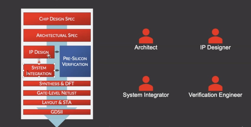
The basic SoC design flow will be reviewed in the webinar, along with the multiple engineering roles that form the design and verification team. Having a way for each of these team members to communicate and collaborate during the project ideation and implementation is crucial for success.

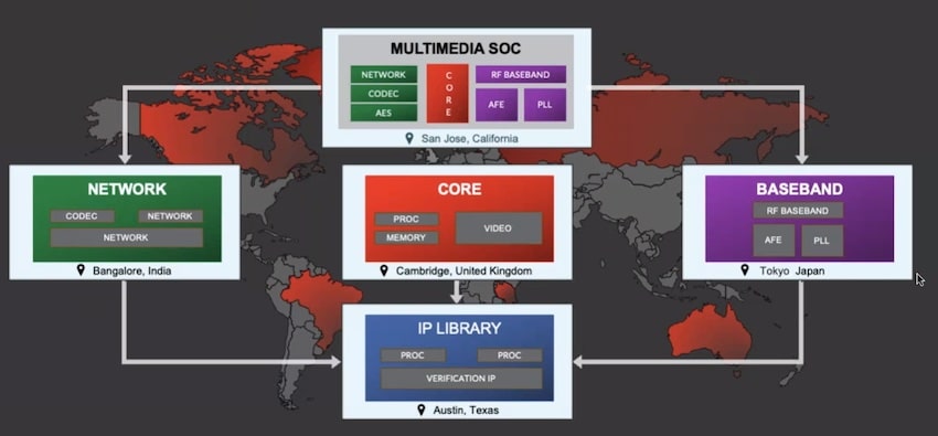
Finding the right IP block either in-house or from third-party vendors is automated with the Keysight IP Management (HUB) tool. System architects typically partition a complex design into smaller pieces using hierarchy as an abstraction, then identify all of the IP blocks required. The members of the design and verification teams may be geographically dispersed, causing communication and documentation challenges. Proper data management tools help with these tasks of partitioning an electronic design, securing the needed IP blocks, and even geofencing IP to conform with license agreements.

In the webinar both the SoC flow and Chiplet design flows are addressed in terms of managing IP and design data. Common challenges for system design include managing the BOM, IP version conflict resolution, assembly of IP subsystems, safely connecting IP blocks to a NoC, reusing design knowledge of connecting to NoCs.
A team member may update the status of an IP block by attaching a tag to that block, like Verification Ready, then automatically informing other team members of the status change, so everyone knows the history and sequence of who has worked on each IP block, and what the next step is in the design flow. An engineer may tag an IP block as RTL Signoff, then a workflow triggers a snapshot or version made of that hierarchy used for future audits, and finally sends emails to all stake holders. Industries like the DOD and Aerospace have rigorous requirements on tracking specifications and requirements into implementation, so running audits is required for traceability.
Legal teams are also interested in knowing which IP is included in every design that is shipped, so that they can properly manage contract agreements for licensed IP blocks.
The Cliosoft tools are fully integrated in the Keysight EDA tool flow, along with IC tool flows from Cadence and Synopsys. EDA tool users stay within their favorite vendor tool to access all the Data Management (DM) features, making for a quick learning curve. Project management tools like Jira are also integrated, along with bug tracking tools like Bugzilla.
Summary
Attend the webinar on November 1 at 10:00AM PT to learn more about data and IP management, even managing the engineering lifecycle from chip specification all the way to tapeout. Both SoC and chiplet design approaches benefit from using automation beyond what a typical PLM system can provide.
Related Blogs
- Keysight EDA 2024 Delivers Shift Left for Chiplet and PDK Workflows
- Version Control, Data and Tool Integration, Collaboration
- Keysight EDA visit at #60DAC
- Keysight at #60DAC
- Keysight Expands EDA Software Portfolio with Cliosoft Acquisition


Comments
There are no comments yet.
You must register or log in to view/post comments.