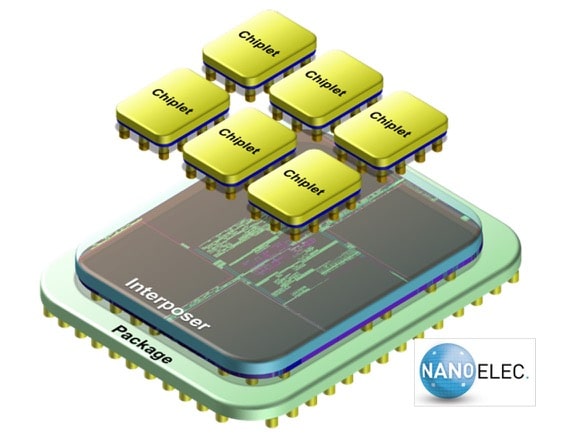
Before chiplets arrived, it seemed like designing an electronic system was a bit simpler, as a system on chip (SoC) methodology was well understood, and each SoC was mounted inside a package, then the packages for each component were interconnected on a printed circuit board (PCB). The emerging trend to design a 3D IC using chiplets has been shown for central processing units (CPU), application processors (AP), graphical processing units (GPU), and even AI chips. With a 3D IC approach there is a promise of higher systems integration, performance improvements, and at a lower cost than using a single SoC.
New challenges arise with a 2.5D or 3D IC design, like knowing how to divide up the system features into chiplets, and then choosing an architecture that will meet requirements: power, performance, area, time to market, cost. Siemens EDA has written a 14 page eBook: Launching the full potential of 3D IC with front-end architectural planning, and I’ll share the major points learned.

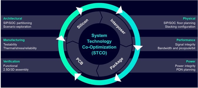
Design-technology co-optimization (DTCO) has been a collaborative process between foundry engineers and IC design engineers to optimize IC metrics, although this is reaching diminishing returns with the slowing of Moore’s Law on the process side. System-technology co-optimization (STCO) takes into account architectural and technology trade-offs earlier in time, and with predictive analysis there are more design scenarios looked at.
Using STCO there is partitioning of hardware and software, where hardware is divided into SoCs or system in package (SIP) using 2.5D or 3D assembly. Heterogenous integration is when multiple chiplets are combined. Collaboration for a chiplet-based approach require early discussions between engineering groups:
- System
- RTL
- Packaging
- Silicon
- Testing

Partitioning hardware into chiplets brings new technical challenges, like:
- Signal Integrity (SI) between chiplets
- Power Integrity (PI) inside the packaging
- Electro-Migration (EM) of interconnect between chiplets
- Thermo-Mechanical stress analysis
- Substrate Verification
- Assembly Verification
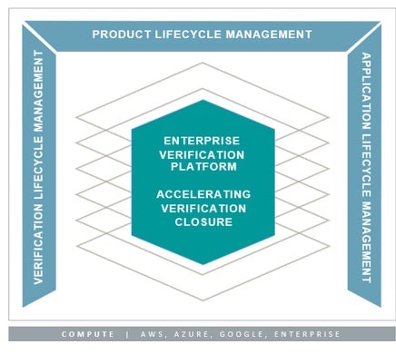
Siemens EDA has a design flow for systems using chiplets and STCO, where you can make early trade-offs and explore how a system is composed. Testbenches can be automatically generated, in only minutes, making your design verification team productive. Verification IP helps engineering teams validate compliance to many industry standards, like:
- PCI Express Gen 6
- Compute Express Link (CXL)
- DDR5
- HBM memory interface protocols
- Flash
- MIPI
- USB
- Ethernet
- Serial
- USB

UCIe
In March 2022 the Universal Chiplet Interconnect Express (UCIe) consortium was announced to support chiplet standards, and the 10 founding member companies are: AMD, Arm, Advanced Semiconductor Engineering, Google Cloud, Intel, Meta, Microsoft, Qualcomm, Samsung and TSMC. UCIe maps PCI Express (PCIe) and CXL protocols, and a standard way for die-to-die communication. Chiplet teams do not have to reinvent the wheel with their own, one of a kind interconnect, instead they can adopt the UCIe standard. There are other interconnects to consider: XSR, USR, AIB, BOW.
Apple M1 Ultra
Apple is at the vanguard of using chiplets for their laptops and tablets, as the M1 Ultra processor chip includes two M1 Max chiplets, connecting 10,000 signals along a single edge. This level of system integration in a package supports 2.5 TB/s of bandwidth, along with eight memory chips, plus an application processor and GPU included.
Summary
Siemens EDA has long been in the systems engineering space, and the 2.5D and 3D trend is also supported for SIP, including architectural design, RTL verification, IP for verification, and support for standards like UCIe. Heterogeneous integration is making the news, and design teams can also catch the wave by choosing a vendor like Siemens EDA.
View the 14 page eBook online.
Related Blogs
- DFT Moves up to 2.5D and 3D IC
- 3D IC – Managing the System-level Netlist
- Three Ways to Meet Manufacturing Rules in Advanced Package Designs
- Five Key Workflows For 3D IC Packaging Success
- Delivering 3D IC Innovations Faster
- CXL Verification. A Siemens EDA Perspective
- Standardization of Chiplet Models for Heterogeneous Integration
- 3D IC Update from User2User
- Joseph Sawicki of Siemens EDA at User2User
- SIP Modules Solve Numerous Scaling Problems – But Introduce New Issues
- System Technology Co-Optimization (STCO)
- Machine Learning Applied to IP Validation, Running on AWS Graviton2
Share this post via:


Comments
There are no comments yet.
You must register or log in to view/post comments.