You are currently viewing SemiWiki as a guest which gives you limited access to the site. To view blog comments and experience other SemiWiki features you must be a registered member. Registration is fast, simple, and absolutely free so please,
join our community today!
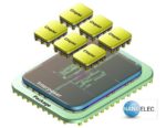
In the 3D-IC (Three-dimensional integrated circuit) chip design method, chiplets or wafers are stacked vertically on top of each other and are connected using Through Silicon Vias (TSVs) or hybrid bonding.
The 2.5D-IC design method places multiple chiplets alongside each other on a silicon interposer. Microbumps and interconnect… Read More
Before chiplets arrived, it seemed like designing an electronic system was a bit simpler, as a system on chip (SoC) methodology was well understood, and each SoC was mounted inside a package, then the packages for each component were interconnected on a printed circuit board (PCB). The emerging trend to design a 3D IC using chiplets… Read More
I attended the 3D architectures for semiconductor integration and packaging conference just before Christmas. I learned a lot and have put together an overview of what is going on in 3D ICs. This is not intended for experts (and if I’ve made egregious errors then please correct them in the forum) but more for people who are … Read More