
Electronics noise is often described as “white,” spread evenly across a band, typical on older semiconductor processes where thermal and shot noise dominate. As transistors shrink, “pink” 1/f noise takes over at low frequencies – becoming stronger in advanced processes and quantum computing technology. But it’s not an easy thing to characterize. Measurement time is bound by slow sampling at low frequencies, while other noise sources factor in across wider device bandwidths. Now, there’s a new approach to seeing 1/f noise more accurately.
The shape of noise depends on its source
In frequency domain over a narrow bandwidth, white noise may look flat – thus the term noise floor. But stretch the bandwidth out from near-DC to high frequencies, and noise takes on a shape, with different contributions from different types of noise. Contributors include:
- Thermal noise comes from the Brownian motion of electrons through resistance, showing up as white noise extending across the analog bandwidth.
- Shot noise happens when electrons flow discontinuously between semiconductor P-N junctions, adding to the white noise profile.
- Random telegraph noise (RTN), or burst noise, comes from small voltage or current transitions due to charge trapping. RTN shows up with 1/f2 power spectral density at near-DC frequencies, sometimes called “red” noise.
- 1/f noise is also caused by charge trapping and is usually more prominent than other sources if manufacturing process quality is high. While strongest at near-DC frequencies, 1/f noise can add noise energy up to a corner frequency.

Additionally, two external noise sources can affect 1/f noise measurements. The first is chamber noise, usually optimized by probe station manufacturers. The second is environmental noise, from sources such as AC power line noise, ground loops in cabling, and nearby equipment – all mitigatable through electromechanical best practices.
Decimation chain speeds up 1/f noise measurements
An OEM’s system noise floor profile affects metrics like signal-to-noise ratio (SNR), receiver sensitivity, and error vector magnitude (EVM). For a low system noise floor, low 1/f noise components are a must. Both passive and active device manufacturers can turn to a low frequency noise analyzer for characterizing parts, improving their performance, and extracting device models for customer use in system simulations.
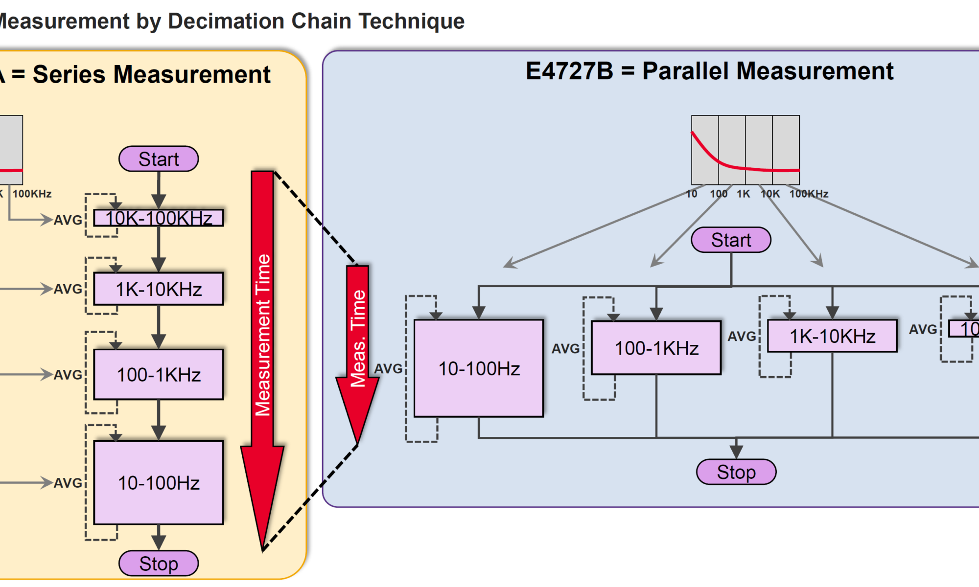
1/f noise measurement has been a different process from wideband noise measurement. One reason is the sheer amount of time a 1/f measurement takes at low frequencies. A good measurement requires a lot of samples and averaging, and as analysis frequencies drop, sample times turn into minutes or longer. This pushed many manufacturers into two different noise measurement instruments, one for low frequencies, one for a wider analog bandwidth. But this approach has twice the test setups and disparate test data from instruments with different noise floors, settings, and algorithms.
One instrument, one test setup, and complete noise results from near-DC to the maximum analog bandwidth sounds great. The question is, how? Keysight looked at the problem differently and came up with the idea of a decimation chain. In short, it takes one set of samples and decimates down to the lowest frequency band. Instead of resampling data for higher frequency bands, it reuses the same samples and runs decimation, FFTs, and averaging on bands in parallel. The result is a solid 1/f noise measurement with major time savings and no reduction in quality.

Turnkey full wafer-level characterization
One core feature of the Keysight E4727B A-LFNA is its ability to see very low noise in devices, such as MOSFET linear region noise. With a system noise floor of 1e-28A^2/Hz and a 1/f noise corner frequency of 15 Hz, plus a maximum analog bandwidth of 100 MHz, the E4727B improves noise characterization. Combining a low noise floor with a wider analysis bandwidth and faster measurement speed makes the E4727B a world-class solution.
When paired with the Keysight WaferPro Express measurement platform and a wafer probing solution like the CM300xi-ULN from FormFactor, the E4727B A-LFNA provides turnkey measurement of DC characteristics, 1/f noise and RTN, and data analysis. Applications include mass characterization of noise specifications for devices on-wafer before packaging, and manufacturing statistical process control.
Another important application is developing process design kits (PDKs). Many firms designing low noise semiconductors are fabless, turning to foundries for wafer fabrication services. The transistors in those foundry processes aren’t under designer control – they’re offered as part of libraries chip designers can choose from. Understanding their characteristics is vital to design success. Adding the Keysight PathWave Model Builder (MBP) or PathWave Device Modeling (IC-CAP) to the suite automates 1/f noise model parameter extraction and model library generation. A foundry can characterize transistors and other primitives in their processes and make 1/f noise data and models available for customers during their evaluation and design workflow.

Seeing 1/f noise more accurately takes on greater importance as transistors get smaller and faster on advanced process nodes. The idea that wafer-level characterization can screen large numbers of devices quickly is powerful. Plus, savings in measurement speed and test setups from using a Keysight E4727B A-LFNA translates to more wafer throughput.
Share this post via:


Comments
There are no comments yet.
You must register or log in to view/post comments.