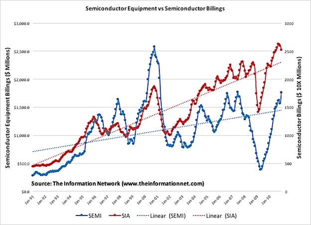
You are currently viewing SemiWiki as a guest which gives you limited access to the site. To view blog comments and experience other SemiWiki features you must be a registered member. Registration is fast, simple, and absolutely free so please,
join our community today!
WP_Term Object
(
[term_id] => 386
[name] => Semiconductor Services
[slug] => semiconductor-services
[term_group] => 0
[term_taxonomy_id] => 386
[taxonomy] => category
[description] =>
[parent] => 0
[count] => 1110
[filter] => raw
[cat_ID] => 386
[category_count] => 1110
[category_description] =>
[cat_name] => Semiconductor Services
[category_nicename] => semiconductor-services
[category_parent] => 0
[is_post] =>
)
This year the Advanced Lithography Conference felt very different to me than the last couple of years. I think it was Chris Mack who proclaimed it the year of Stochastics. EUV has dominated the conference for the last several years but in the past the conversation has been mostly centered on the systems, system power and uptime.
I … Read More
The global semiconductor market grew 21.6% for the year 2017, according to World Semiconductor Trade Statistics (WSTS). The market was much stronger than anticipated at the beginning of year. Semiconductor Intelligence tracked publicly available forecasts to determine which was the most accurate. We used forecasts made … Read More
I was invited to present at Nikon’s LithoVision event held the day before the SPIE Advanced Lithography Conference in San Jose. The following is a write up of the talk I gave. In this talk I discuss the three main segments in the semiconductor industry, NAND, DRAM and Logic and how technology transitions will affect lithography.… Read More
Years ago my good friend Herb Reiter promoted the importance of 2.5D packaging to anybody and everybody who would listen including myself. Today Herb’s vision is in production and the topic of many papers, webinars, and conferences. According to Herb, and I agree completely, advanced IC packaging is an important technology for… Read More
There’s been a lot of discussion of late about deep learning technology and its impact on many markets and products. A lot of the technology under discussion is basically hardware implementations of neural networks, a concept that’s been around for a while.
What’s new is the compute power that advanced semiconductor technology… Read More
High Bandwidth Memory (HBM) systems have been successfully used for some time now in the network switching and high-performance computing (HPC) spaces. Now, adding fuel to the HBM fire, there is another market that shares similar system requirements as HPC and that is Artificial Intelligence (AI), especially AI systems doing… Read More
If you are interested in what types of chips we will see in the coming years always ask an ASIC provider because they know. Companies of all sizes (small-medium-large) use ASIC companies to get their chips out in the least amount of time and at a minimum cost because that is what ASIC companies do.
IP is an important ingredient to the … Read More
One of the other blog worthy analyst presentations at ISS 2018 was by Len Jelinek of IHS. Len is my kind of analyst, he spent 28 years in the semiconductor industry before going to the dark side so he knows what he is talking about. Len’s presentation on Global Semiconductor Market Trends is action packed so I will be doing a lot of cut … Read More
As I have said many times, IEDM is one of the premier conferences for semiconductor technology. On Sunday before the formal conference started I took the “Boosting Performance, Ensuring Reliability, Managing Variation in sub-5nm CMOS” short course. The second module in the course was “Multi-Vt Engineering… Read More
DAC 2018 will take place in San Francisco in June (24 to 28) and you have a fantastic opportunity to present a paper in the IP track! In fact, the deadline has been extended to January 30[SUP]th[/SUP] to submit your proposal.
Let’s make it clear: you are not expected to send the completed paper by this date, just the following:
…
Read More
Rethinking Multipatterning for 2nm Node