You are currently viewing SemiWiki as a guest which gives you limited access to the site. To view blog comments and experience other SemiWiki features you must be a registered member. Registration is fast, simple, and absolutely free so please,
join our community today!
            WP_Term Object
(
    [term_id] => 24
    [name] => TSMC
    [slug] => tsmc
    [term_group] => 0
    [term_taxonomy_id] => 24
    [taxonomy] => category
    [description] =>
    [parent] => 158
    [count] => 642
    [filter] => raw
    [cat_ID] => 24
    [category_count] => 642
    [category_description] =>
    [cat_name] => TSMC
    [category_nicename] => tsmc
    [category_parent] => 158
    [is_post] =>
)

WP_Term Object
(
    [term_id] => 24
    [name] => TSMC
    [slug] => tsmc
    [term_group] => 0
    [term_taxonomy_id] => 24
    [taxonomy] => category
    [description] =>
    [parent] => 158
    [count] => 642
    [filter] => raw
    [cat_ID] => 24
    [category_count] => 642
    [category_description] =>
    [cat_name] => TSMC
    [category_nicename] => tsmc
    [category_parent] => 158
    [is_post] =>
)
L.C. leads efforts in design enablement, ensuring that the company can meet the diverse and evolving requirements of its global customer base. Prior to this, he headed the Design and Technology Platform organization starting in 2018.
Since joining TSMC in 2000, Dr. Lu has held multiple leadership positions in design services.… Read More
Dr. Y.J. Mii joined TSMC in 1994 as a manager at Fab 3 before moving into the company’s research and development organization in 2001. He was appointed Vice President of R&D in 2011 and later advanced to Senior Vice President in November 2016.
Over more than 20 years at TSMC, Dr. Mii has played a central role in advancing and manufacturing… Read More
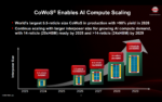
The rapid rise of artificial intelligence is fundamentally reshaping computing architectures. As AI models scale toward trillions of parameters, traditional approaches to performance improvement are no longer sufficient. Instead, the industry is entering a new era where system-level innovation, advanced packaging, … Read More
Before assuming his current position, Dr. Hou held several key leadership roles. He served as Vice President of Design and Technology Platform from 2011 to 2018, and later as Vice President of Technology Development starting in August 2018. Earlier in his career, from 1997 to 2007, he established TSMC’s technology design kit
…
Read More
At its 2026 Technology Symposium, TSMC delivered a clear message: the AI era has entered a new phase. The primary constraint is no longer model capability, but the systems required to run those models at scale. Addressing this shift will demand significant advances in semiconductor technology, spanning compute, memory, interconnects,… Read More
The rapid evolution of wireless audio has placed unprecedented demands on system integration, power efficiency, and performance. Against this backdrop, the webinar “All-in-One Bluetooth Audio: A Complete Solution on a TSMC 12nm Single Die” offers a timely and technically rich exploration of how modern semiconductor design… Read More
Yes, it is that time of year again, the 2026 TSMC Technology Symposium kick-off event in Silicon Valley. TSMC has never been in a better position to forecast the future of semiconductor technology and the industry itself. TSMC closely collaborates with the top semiconductor companies around the world and the top players in the … Read More
The opening of the TSMC 2026 earning call series brought no surprises. CC Wei has done more than 30 such calls since taking the CEO position in 2018 and he never fails to disappoint. Once again, CC Wei reported numbers above guidance driven by strong demand and flawless execution. This illustrates the benefit of TSMC’s close collaborations… Read More
One of my favorite times of the year is coming (sailing season) and my favorite event of the year is coming as the company I most respect will host the best international semiconductor networking event starting here in Silicon Valley.
The 32nd annual TSMC Technology Symposium represents one of the most influential events in the … Read More
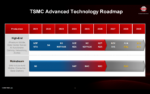
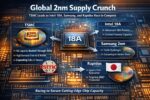
The semiconductor industry is in the midst of a structural supply challenge that’s tightly coupled to exploding demand for advanced chips, especially those used in AI, HPC, and next-generation mobile and consumer devices. At the center of this vortex is the 2nm class of manufacturing technology, representing one of the most … Read More