You are currently viewing SemiWiki as a guest which gives you limited access to the site. To view blog comments and experience other SemiWiki features you must be a registered member. Registration is fast, simple, and absolutely free so please,
join our community today!
            WP_Term Object
(
    [term_id] => 18
    [name] => Intel Foundry
    [slug] => intel
    [term_group] => 0
    [term_taxonomy_id] => 18
    [taxonomy] => category
    [description] =>
    [parent] => 158
    [count] => 469
    [filter] => raw
    [cat_ID] => 18
    [category_count] => 469
    [category_description] =>
    [cat_name] => Intel Foundry
    [category_nicename] => intel
    [category_parent] => 158
    [is_post] =>
)

WP_Term Object
(
    [term_id] => 18
    [name] => Intel Foundry
    [slug] => intel
    [term_group] => 0
    [term_taxonomy_id] => 18
    [taxonomy] => category
    [description] =>
    [parent] => 158
    [count] => 469
    [filter] => raw
    [cat_ID] => 18
    [category_count] => 469
    [category_description] =>
    [cat_name] => Intel Foundry
    [category_nicename] => intel
    [category_parent] => 158
    [is_post] =>
)
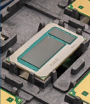
Chiplets (die stacking) is not new. The origins are deeply rooted in the semiconductor industry and represent a modular approach to designing and manufacturing integrated circuits. The concept of chiplets has been energized as a response to the recent challenges posed by the increasing complexity of semiconductor design. … Read More
The annual International Electron Devices Meeting (IEDM) took place last month. One of the presentations on the short course was by Matthew Metz of Intel titled New Materials Systems for Moore’s Law Continuation. In essence this was a look at some of the possibilities for what comes after silicon runs out of steam.
Matthew started… Read More
There is a lot being said about Intel getting the lead back from TSMC with their 18A process. Like anything else in the semiconductor industry there is much more here than meets the eye, absolutely.
From the surface, TSMC has a massive ecosystem and is in the lead as far as process technologies and foundry design starts but Intel is … Read More
For more than 65 years, the IEEE International Electron Devices Meeting (IEDM) has been the world’s pre-eminent forum for reporting technological breakthroughs in the areas of semiconductor and electronic device technology, design, manufacturing, physics, and modeling. As I post this, the conference is underway in San Francisco… Read More
Intel recently issued a press announcement that has significant implications for the future of semiconductors. The release announces Intel’s new glass substrate technology. The headline states: Glass substrates help overcome limitations of organic materials by enabling an order of magnitude improvement in design rules… Read More
Given the changes in the music business, the term “Rock Star” doesn’t really have any relevance to music or its performers anymore. Instead, we use the term to describe leaders, innovators and generally people or organizations of great significance. In the world of semiconductors, the designers of advanced chips were the rock… Read More
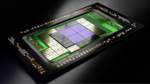
The trend is undeniable. Highly integrated monolithic chips can no longer handle the demands of next-generation systems. The reasons for this significant shift in design are many. Much has been written on the topic; you can get a good overview of the forces at play in multi-die design here. These changes represent the next chapter… Read More
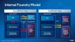
Intel held a webinar today to discuss their IDM2.0 internal foundry model. On the call were Dave Zinsner Executive Vice President and Chief Financial Officer and Jason Grebe Corporate Vice President and General Manager of the Corporate Planning Group.
On a humorous note, the person moderating the attendee questions sounded … Read More
(First published December 24, 2014)
A list of the best and worst CEOs in 2014 was recently published. The good news is that none of our semiconductor CEOs were on the worst list. The bad news is that none of our semiconductor CEOs were on the best list either. I will be writing about the CEOs that made our industry what it is today starting… Read More
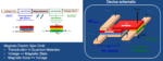
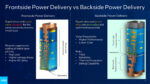
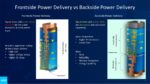
At the 2023 VLSI Symposium on Technology and Circuits, Intel presented two papers on their PowerVia technology. We received a pre-conference briefing on the technology embargoed until the conference began and received the papers.
Traditionally all interconnects have taken place on the front side of devices with signal and … Read More