You are currently viewing SemiWiki as a guest which gives you limited access to the site. To view blog comments and experience other SemiWiki features you must be a registered member. Registration is fast, simple, and absolutely free so please,
join our community today!
WP_Term Object
(
    [term_id] => 50
    [name] => Events
    [slug] => events
    [term_group] => 0
    [term_taxonomy_id] => 50
    [taxonomy] => category
    [description] =>
    [parent] => 0
    [count] => 1516
    [filter] => raw
    [cat_ID] => 50
    [category_count] => 1516
    [category_description] =>
    [cat_name] => Events
    [category_nicename] => events
    [category_parent] => 0
    [is_post] =>
)
After the onslaught of IoT devices Christmas brought to the masses we really need to talk about security or lack thereof. Do me a favor and count how many IoT devices you have now? Our house IoT count is probably a bit higher than average due to my technology addiction but we are firmly in the double digits and the security breach stories… Read More
While writing the definitive book on ARM history we could not have imagined a more different exit than the SoftBank acquisition, not even close. It is now very clear why SoftBank acquired ARM for $31B. It is also very clear why alternatives like RISC-V are trending on SemiWiki and will continue to do so, absolutely. No matter what … Read More
When Nvidia changed its automotive market messaging from an infotainment-centered theme to autonomous driving two years ago – pronouncing the coming tidal wave of robotaxi development – it matched the almost identical epiphany reached by Intel years prior. Automotive infotainment is a low volume, low revenue… Read More
The annual trek to Las Vegas arrives this year with visions of sinusitis, chapped lips, flat feet and new concepts for automotive cockpit systems. It is no coincidence that the plaza in front of the Las Vegas Convention Center is dominated by automotive exhibits – along with multiple automated driving demonstrations across the… Read More
Attendees of CES 2019 arriving at Las Vegas McCarran International Airport next week will have four options for getting to their hotels: a shuttle offering two rides for the price of one (out and back for about $15); a taxi offering one ride for the price of two (about $30), a Lyft or Uber offering one ride for the price of one ride (about… Read More
As I mentioned in a previous post, the big drama at last year’s Design Automation Conference was the acquisition of the Electronic Systems Design Alliance (formerly EDAC) by SEMI, the owner of the SEMICON West Conference franchise. The plan is to add an ES Design West wing to the SEMICON West conference in San Francisco next year.… Read More
As 2018 wraps up this month it’s time to start thinking and planning for 2019, and if you work in the Silicon Valley then you’ll want to consider adding the 31st annual DVCon event planned for February 25-28 in San Jose. Surveys have shown for some time now that verification tasks actually take up more time on a SoC project… Read More
IEDM 2018 Trip Report!by Daniel Nenni on 12-10-2018 at 7:00 amCategories: Events
Hello, my name is Daniel Nenni and I am a semiconductor conference addict. I just can’t seem to get enough. The semiconductor ecosystem is very wide now and moves so quickly it is nearly impossible to keep up without constant conference attendance. As a SemiWiki contributor not only do I get free conference passes, I get access to … Read More
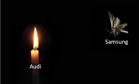
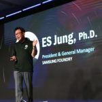
IEDM is a premier semiconductor conference so it was certainly appropriate for Samsung to do the keynote since they are the largest and one of the most innovative semiconductor companies in the world, absolutely.
Samsung is also one of the more interesting semiconductor companies since they do it all: chip design, semiconductor… Read More
Cadence held a well-attended Automotive Summit where Cadence presented an overview of their solution and system enablement along with industry experts and established or startup companies sharing their perspective and product features from autonomous driving, LiDAR, Radar, thermal imaging, sensor imaging, and AI.… Read More


Captain America: Can Elon Musk Save America’s Chip Manufacturing Industry?