The electromagnetism problems upon which we spent many hours laboring away on homework in college has a mathematical formulation originally developed by Maxwell, Lorentz, Gauss, Faraday and others. In their full forms, these formulas are partial differential equations that come in many versions – both differential and integral.… Read More
Leveraging Virtual Platforms to Shift-Left Software Development and System Verification
Ever since the cost of development started growing exponentially, engineering teams have been deploying a shift-left strategy to software development and system verification. While this has helped contain cost and accelerated product development schedules, a shift-left strategy is not without challenges. A virtual platform… Read More
Webinar: From Glass Break Models to Person Detection Systems, Deploying Low-Power Edge AI for Smart Home Security
Moving deep learning from the cloud to the edge is the holy grail when it comes to deploying highly accurate, low-power applications. Market demand for edge AI continues to grow globally as new hardware and software solutions are now more readily available, enabling any sized company to easily implement deep learning solutions… Read More
Webinar: Beyond the Basics of IP-based Digital Design Management
According to the ESD Alliance, the single biggest revenue category in our industry is for semiconductor IP, so the concept of IP reuse is firmly established as a way to get complex products to market more quickly and reducing risk. On the flip side, with hundreds or even thousands of IP blocks in a complex SoC, how does a team, division… Read More
WEBINAR: Balancing Performance and Power in adding AI Accelerators to System-on-Chip (SoC)
Among the multiple technologies that are poised to deliver substantial value in the future, Artificial Intelligence (AI) tops the list. An IEEE survey showed that AI will drive the majority of innovation across almost every industry sector in the next one to five years.
As a result, the AI revolution is motivating the need for … Read More
Breker Verification Systems Unleashes the SystemUVM Initiative to Empower UVM Engineering
The much anticipated (virtual) DVCON 2022 is happening this week and functional verification plus UVM is a very hot topic. Functional Verification Engineers using UVM can enjoy a large number of benefits by synthesizing test content for their testbenches. Abstract, easily composable models, coverage-driven content, deep… Read More
Intel 2022 Investor Meeting
Last Thursday Intel held their investors meeting, in this write up I wanted to focus on my areas of coverage/expertise, process technology and manufacturing.
Technology Development presented by Ann Kelleher
Last year Intel presented their Intel Accelerated plan and, in this meeting, we got a review of where Intel stands on that… Read More
Semiconductor Earnings Roundup
ON, ACLS, RMBS, AOSL, CAMT, ICHR, ONTO, SUMCO, and more!
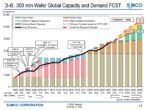
SUMCO was the best call I read this quarter. There were many great bits of information but I want to start with the stat that really shocked me.
First of all, with regard to the LTAs out to 2026 and whether we did make progress in the last 3 months, that is correct. In the last 3 months,
AMAT – Supply Constraints continue & Backlog Builds- Almost sold out for 2022
-Production constraints push backlog up $1.3B to $8B
-Looks like $100B in WFE 2022 VS $80B in 2021
-Almost sold out for 2022- Could lead to continued growth 2023
-Insp/metrology up 68% Y/Y- Expect steady growth in 2022
Can’t keep up with demand….
Revenue came in at $6.27B and NonGAAP EPS of $1.89. A very slight beat of … Read More
Tower Semi Buyout Tips Intel’s Hand
The rationale behind the Tower Semi acquisition and things to watch out for at Intel’s investor day.
Intel bids for Tower Semi
First I have to quote myself because Tower was an error of omission. In November in a piece that was likely too long for its own good, I mentioned that trailing edge fabs are in a huge position of strength… Read More


Musk’s Orbital Compute Vision: TERAFAB and the End of the Terrestrial Data Center