The annual SPIE Advanced Lithography Conference kicked off last night with vendor sponsored networking events and such. SPIE is the international society for optics and photonics but this year SPIE Advanced Lithography is all about the highly anticipated EUV technology. Scotten Jones and I are at SPIE so expect more detailed… Read More

Webinar: FPGA Prototyping and ASIC Design
When you think about working with an ASIC service provider like Open-Silicon, you probably think about handling all the architecture, design and verification/validation in your shop, handing over a netlist and some other collateral, then the ASIC services provider takes responsibility for implementation and manufacturing.… Read More
Another Live Event at Samsung!
Last week Samsung hosted the GSA Silicon Valley “State of the Industry” Meet-up which was well attended by the semiconductor elite, myself included. The agenda started with an update on the semiconductor industry outlook followed by deep dives into Automotive, IoT, Artificial Intelligence, and Cybersecurity all of which are… Read More
What You Don’t Know about Parasitic Extraction for IC Design
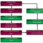
Out of college my first job was doing circuit design at the transistor-level with Intel, and to get accurate SPICE netlists for simulation we had to manually count the squares of parasitic interconnect for diffusion, poly-silicon and metal layers. Talk about a burden and chance for mistakes, I’m so thankful that EDA companies… Read More
"Ten-hut!" Attending the Signal Integrity Bootcamp

The engineering team for the design and analysis of a complex system consists of a diverse set of skills — with the increasing emphasis on both high-speed interface design and multi-domain power management, a critical constituent of the team is the group of signal integrity (SI) and power integrity (PI) engineers.
The training… Read More
Mentor gets Busy at DVCon

You’d expect Mentor to be covering a lot of bases at DVCon and you wouldn’t be wrong. They’re hosting tutorials, a lunch, papers, posters, there’s a panel and of course they’ll be on the exhibit floor. I’ll start with an important tutorial that you really should attend, Monday morning, on creating Portable Stimulus Models… Read More
Four Barriers to Using an SoC for IoT Projects
I often read about the large number of expected IoT design starts around the world, so I started to think about what the barriers are for launching this industry in order to meet the projections. One of my favorite IoT devices is the Garmin Edge 820, a computer for cyclists that has sensors for speed, cadence, power, heart rate, altitude… Read More
DVCon San Jose February 27th – March 2nd
DVCon is fast approaching, less than 3 weeks away. As a verification geek, this must be one of my favorite conferences, so I’ll be there; you’ll see me at tutorials, presentations and wandering around the Exhibit hall. (Pictures here from the 2016 DVCon – many of the same attendees will be at this year’s conference after all :cool:)… Read More
Scott Jones ISS Talk – Moore’s Law Lives!
I was invited to give a talk at this year’s ISS conference, the talk seemed to be very well received and I was asked to blog about it for SemiWiki. Parts of the talk will be familiar to SemiWiki readers from some of my previous blogs but I also went into more detail around some scaling challenges. The following is a summary of what… Read More
SPIE Advanced Lithography and Synopsys!

SPIE is the premier event for lithography held in Silicon Valley and again Scotten Jones and I will be attending. EUV is generally the star of the show and this year will be no different now that TSMC has committed to EUV production in 2019.
Last year at SPIE, TSMC presented the history of EUV development from the beginning in 1985 as … Read More
The Silicon Shield Has Never Been Stronger!