A vital benefit of advanced EM simulations is their ability to take on complicated physical test setups, substituting far easier virtual tests yielding accurate results earlier during design activities. The latest release of Keysight PathWave ADS 2023 continues speeding up engineering workflows. Let’s look at three… Read More

Electronic Design Automation
Three Ways to Meet Manufacturing Rules in Advanced Package Designs

Often designers are amazed at the diversity of requirements fabricators and manufacturers have for metal filled areas in advanced package designs. Package fabricators and manufacturers do not like solid metal planes or large metal areas. Their strict metal fill requirements address two main issues. The dielectric and metal… Read More
Synopsys Vision Processor Inside SiMa.ai Edge ML Platform

SiMa.ai just announced that they achieved first silicon success on their new MLSoC, for AI applications at the edge, using Synopsys’ design, verification, IP and design services solutions. Notably this design includes the Synopsys ARC® EV74 processor (among other IP) for vision processing. SiMa.ai claim their platform, now… Read More
Machine Learning in the Fab at #59DAC
It used to be true that a foundry or fab would create a set of DRC files, provide them to designers, and then the process yield would be acceptable, however if the foundry knows more details about the physical implementation of IC designs then they can improve the yield. Using a digital twin of the design, process and metrology steps… Read More
WEBINAR: Scalable, On-Demand (by the Minute) Verification to Reach Coverage Closure
Verification has long been the most time-consuming and often resource-intensive part of chip development. Building out the infrastructure to tackle verification can be a costly endeavor, however. Emerging and even well-established semiconductor companies must weigh the Cost-of-Results (COR) against Time-to-Results
Connecting SystemC to SystemVerilog
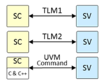
Siemens EDA is clearly on a mission to help verifiers get more out of their tools and methodologies. Recently they published a white paper on UVM polymorphism. Now they have followed with a paper on using UVM Connect, re-introducing how to connect between SystemC and SystemVerilog. I’m often mystified by seemingly overlapping… Read More
Webinar: Semifore Offers Three Perspectives on System Design Challenges
The exponential increase in design complexity is a popular topic these days. In fact, it’s been a topic of discussion for a very long time. The explosion of chip and system design complexity over the past ten years has become legendary and haunts many of us daily. A lot of the complexity we face has to do with coordinating across an ever-increasing… Read More
Today’s SoC Design Verification and Validation Require Three Types of Hardware-Assisted Engines

Lauro Rizzatti offers Semiwiki readers a two-part series on why three kinds of hardware-assisted verification engines are now a must have for semiconductor designs continues today. His interview below with Juergen Jaeger, Prototyping Product Strategy Director in the Scalable Verification Solution division at Siemens EDA,… Read More
Podcast EP105: Cadence STA Strategy and Capabilities, Today and Tomorrow with Brandon Bautz
Dan is joined by Brandon Bautz, senior group director of product management responsible for silicon signoff and verification product lines in the Cadence Digital & Signoff Group. Brandon has more than 20 years of experience in chip design and the EDA industry and has been at Cadence for over 10 years.
Dan explores the current… Read More
Resilient Supply Chains a Must for Electronic Systems

The last few years have seen multiple disruptions in the supply chain in many industries. One of the key technologies that many fingers have pointed to is the semiconductor technology. As products in all industries become more electronics based, semiconductors play a key role since no end system could function today without … Read More
Musk’s Orbital Compute Vision: TERAFAB and the End of the Terrestrial Data Center