
Once upon a time, ASIC designers were integrating memories in their design (using a memory compiler being part of the design tools provided by the ASIC vendor), then they had to make the memory observable, controllable… and start developing the test program for the function, not a very enthusiastic task (“AAAA” and “5555” and other… Read More
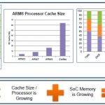
How much SRAM proportion could be integrated in SoC at 20 nm and below?


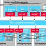

Consolidation and Competition: Who is Winning the $4.5 Billion Interface IP Race?