Ever since I have seen Atrenta’s SpyGlass platform providing a comprehensive set of tools across the semiconductor design paradigm, I felt the need for a common set of standards to evolve for sign-off at RTL level. Last December, when I read an EE Times articleof Piyush Sancheti, VP, Product Marketing at Atrenta, where he talks … Read More

Electronic Design Automation
Power and Thermal Modeling Approach for Embedded and Automotive using ESL Tools
Did you know that an S-class Mercedes Benz can use 100 microprocessor-based electronic control units (ECUs) networking throughout the vehicle that run 20-100 million lines of code (Source: IEEE)?
2014 Mercedes-Benz CLA
Here’s a quick list of all the places that you will find software controlling hardware in an automobile:… Read More
Update on a Space-Based Router for IC Design
When I started my IC design career back in 1978 all IC routing was done manually, today however we have many automated approaches to IC routing that save time and do a more thorough job than manual routing. To get an update on space-based routers for IC design I connected with Yuval Shay at Cadence today. The basic idea behind a spaced-based… Read More
Getting the best from MIPI IP Toolbox
The set of MIPI specifications has severely enlarged during the past year. This is a positive point, as the large set of specifications induces a wider choice, and a chip maker can decide to implement a complex specification to differentiate with competitors, or select a specification just tailored to support a basic architecture… Read More
Untangling snags earlier and reducing area by 10%
The over 20 years of experience behind Synopsys Design Compiler is getting a new look for 2014, and we had a few minutes with Priti Vijayvargiya, director of product marketing for RTL synthesis, to explore what’s in the latest version of the synthesis tool.
Previewed today, Synopsys Design Compiler 2013.12 continues to target … Read More
First Verdi Interoperability Apps Developer Forum

Way back when SpringSoft was still SpringSoft and not Synopsys they launched Verdi Interoperability Apps (VIA) and an exchange for users to share them open-source style. I wrote about it back in 2011 when it was announced. Today, Synopsys announced the first developer forum for VIA. It will be held at SNUG on Wednesday, March 26,… Read More
If requirements ask for it, it had better be there
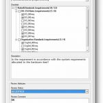
Engineers are known for their attention to detail and precision in thinking, but sometimes still struggle during compliance audits. This is especially true the longer a list of requirements becomes, especially unstructured lists kept in spreadsheets and on Post-It notes.
It gets even more complicated, because in defense circles… Read More
High Quality PHY IPs Require Careful Management of Design Data and Processes
In last few years IP design has grown significantly compared to the rest of the semiconductor industry. There are newer IP start-ups opening across the world, particularly in India and China. Amid this rush, I wanted to understand the actual dynamics pushing this business and whether all of these IPs follow quality standards. … Read More
CDNLive World Tour

CDNLive is becoming a real worldwide event, starting in March in San Jose and ending in November in Tel Aviv, Israel.
The complete schedule is:
- March 11-12th, Santa Clara, California
- May 19th-21st, Munich, Germany
- July 15th, Seoul, Korea
- August 15th, Shanghai, China
- August 7th, Hsinchu, Taiwan
- August 11-12th, Bangalore, India
TSMC OIP presentations available!
Are you a TSMC customer or partner? If so, you’ll want to take a look at these presentations from the 2013 TSMC Open Innovation Platform conference:
- Design Reliability with Calibre YE-SmartFill and Calibre PERC (Broadcom & Mentor Graphics)
New methodologies were developed for 28nm designs using Calibre SmartFill and Calibre
Musk’s Orbital Compute Vision: TERAFAB and the End of the Terrestrial Data Center