Get together with your fellow industry peers and insiders at the monthly EDAC Mixer, to the benefit of local charities. You don’t need to donate anything, you just show up and pay for your own drinks. A portion of the proceeds will go to local charities, this month to the Resource Area for Teaching (RAFT), a San Jose based non-profit… Read More

Electronic Design Automation
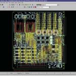
Sketch Router and auto-assist PCB layout
Archaic tech metaphors abound, stuck in the psyche of users everywhere. We still “dial” numbers, long after the benefit of a short pull area code disappeared. (Humans could dial 1, 2, or 3 a lot faster on a rotary phone, and there were fewer dialpulses for central office switches to decode – thus big cities with more phone traffic like… Read More
Sebastian Thrun: Self-driving cars, MOOCs, Google Glass and more

Sebastian Thrun gave a fascinating keynote at SNUG last week. It didn’t have that much to do with IC design but he discussed 3 projects that he had been involved with. Anyone would be happy to have just one of these projects on their resume but he has all these (and more).
The first is the Google self-driving car. This project actually… Read More
Automating Analog Verification in Virtuoso
Digital designers have been automating the functional verification process for many years now, however when you talk to an analog designer about how they do verification you quickly realize that the typical process is quite ad-hoc and little automated. Necessity does create an opportunity so the software engineers at Methodics… Read More
Jasper Announces Sequential Equivalence Checking
Jasper finally announced their sequential equivalence checking app this morning. I say finally because they haven’t really tried to keep it a secret. They talked about it at the end of last year the Jasper User Group meeting and it has even had a page on their website. But formally the product was announced today.
The new JasperGold… Read More
Bye-Bye DDRn Protocol?
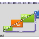
In fact, this assertion is provocative, as the DDR4 protocol standard has just been released by JEDEC… after 10 years discussion around the protocol features. Yes, the first discussions about DDR4 have started ten years ago! Will DDR4 be used in the industry? The answer is certainly yes, and DDR4 will most probably be used for years.… Read More
Social Media at Atrenta
Atrentais well-known for their SpyGlass software that enables SoC engineers to run early design analysis on RTL code and create a hardware virtual prototype for analysis prior to implementation. Visiting their website you quickly see that social media plays an important role in connecting with engineers as links for Facebook,… Read More
Applied Power Electronics Conference & Exposition 2014: "Less Power"
On the television show “Home Improvement”, Tim Allen’s character always sought “more power” for whatever project he was working on. The theme of the Applied Power Electronics Conference and Exposition (APEC) 2014 could have been “less power”. APEC 2014 featured five days of seminars and sessions including professional education,… Read More
IP Challenges, FinFET, 3D-IC, and FD-SOI Updates
Semiwiki is proud to be a sponsor of EDPS 2014:
April 17 & 18, 2014
Monterey Beach Hotel, Monterey, CA
Sponsored by:
IEEE Computer Society of Silicon Valley (CS-SCV)
IEEE Computer Society
Design Automation Technical Committee (DATC)
Council on Electronic Design Automation (CEDA)
The Electronic Design Processes Symposium… Read More
Early RTL Power Analysis and Reduction
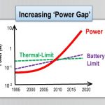
Power analysis and reduction for SoC designs is a popular topic because of our consumer electronics dominated economy, and the need to operate devices on a battery source for the maximum time before a recharge. Just from my desk I can see multiple battery-powered devices: Laptop, tablet, smart phone, e-book reader, bluetooth … Read More
Musk’s Orbital Compute Vision: TERAFAB and the End of the Terrestrial Data Center