In 2014, a Goldman Sachs’ report took many people by surprise when it picked Atmel Corp. as the company best positioned to take advantage of the rising Internet of Things (IoT) tsunami. At the same time, the report omitted tech industry giants like Apple and Google from the list of companies that could make a significant impact… Read More

Electronic Design Automation
A Vision for FPGA Prototyping Realized
FPGA prototyping is beginning its move to the forefront of design and verification. More and more companies are turning to this technology not only for in-circuit testing and earlier software development but also for refining, validating, and implementing chip architecture. The increases in design size and complexity as well… Read More
Growing Innovation in Modern PCB Design Tools

In last 30+ years, the electronic design industry has seen rapid changes more than any other industry. The change has taken place in the whole electronic ecosystem including semiconductor technology, transistor design, IC / SoC design, PCB, and system design. Today, a PCB can be very complex connecting several heterogeneous… Read More
Managing Design Flows in RF Modules
The semiconductor industry is expected to grow at a reasonable pace in 2015 and beyond, with the biggest market being compute applications followed by wireless and consumer applications. The highest growth, however, is expected to be in application-specific products for devices such as smartphones, wearables, memories, … Read More
Shift-West of Semicon Power Centers
It’s true that Japan was once the center of semiconductor business and we were carrying on with that perception until recently. In 1990, six out of top10 semiconductor companies (excluding pure-play foundries) were in Japan; and 59% of worldwide semiconductor market was concentrated with the top10 companies. The semiconductor… Read More
Xtensa Fusion DSP Target IoT including Wireless and Security
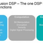
Internet of Things (IoT) can be seen as a fashionable buzzword covering so many distinct applications that IoT is sometimes nick-named “Internet of Everything”, or it can be perceived as the next revolution in electronic systems generating more revenues than the smartphone and computer market together in 2020. But the industry… Read More
CEVA DSP Cores … Inside Intel
Intel Corp. is gaining discernible market share in the LTE chips business, and Qualcomm, the 800-pound gorilla in the mobile baseband market, suddenly looks in Intel’s crosshairs. A closer look at Intel’s journey from a mobile silicon underdog to the owner of a swelling LTE footprint shows that design ingredients… Read More
Are There Trojans in Your Silicon? You Don’t Know

Yesterday was the Mentor users’ group U2U. As usual, Wally Rhines gave the keynote, this year entitled Secure Silicon, Enabler for the Internet of Things. Wally started off saying it was a challenge to find a new angle. The number of news articles on cloud computing has exploded from nothing to 72,000 last year. On IoT from … Read More
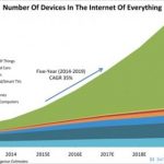
How is Trillion Sensors by 2025 Panning Out?
From several literatures, talks in the semiconductor industry, forecasts, and BHAGs (Big Hairy Audacious Goals), specifically in the context of IoT (Internet of Things) and IoE (Internet of Everything), we have been looking forward to a world with over a trillion sensors around us. I recollect (produced below) from an impressive… Read More
S2C eyeing 1B gate FPGA-based prototypes
We hear a lot about FPGA-based prototyping hardware: Aldec, Dini Group, PRO DESIGN, Synopsys, and others. So, why is today’s news on a new platform from S2C important? It’s a matter of intent, beyond the act of gluing a few large FPGAs on a board for customers to dump more and more prospective RTL into.
Size differences aside, each … Read More
Silicon Insurance: Why eFPGA is Cheaper Than a Respin — and Why It Matters in the Intel 18A Era