You are currently viewing SemiWiki as a guest which gives you limited access to the site. To view blog comments and experience other SemiWiki features you must be a registered member. Registration is fast, simple, and absolutely free so please,
join our community today!
WP_Term Object
(
    [term_id] => 157
    [name] => EDA
    [slug] => eda
    [term_group] => 0
    [term_taxonomy_id] => 157
    [taxonomy] => category
    [description] => Electronic Design Automation
    [parent] => 0
    [count] => 4514
    [filter] => raw
    [cat_ID] => 157
    [category_count] => 4514
    [category_description] => Electronic Design Automation
    [cat_name] => EDA
    [category_nicename] => eda
    [category_parent] => 0
    [is_post] =>
)
By Marko Suominen and Slava Zhuchenya of Siemens Digital Industries Software.
It’s often said that an orchestra without a conductor is just a collection of talented individuals making noise. The conductor’s role is to transform that potential cacophony into a unified, beautiful symphony. The same concept holds… Read More
Wednesday was the last day at #62DAC for me and I attended an Exhibitor Session entitled, Engineering the Semiconductor Digital Thread, which featured Vishal Moondhra, VP Solutions Engineering of Perforce IPLM and Michael Munsey, VP Semiconductor Industry at Siemens Digital Industries. Instead of just talking from slides,… Read More
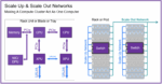
The evolution of hyperscale data center infrastructure to support the processing of trillions of parameters for large language models has created some rather substantial design challenges. These massive processing facilities must scale to hundreds of thousands of accelerators with highly efficient and fast connections.… Read More
This time let’s see if we can stir up some lively debate. Cocotb isn’t new but it is an interesting alternative to mainstream testing methodologies. Paul Cunningham (GM, Verification at Cadence), Raúl Camposano (Silicon Catalyst, entrepreneur, former Synopsys CTO and lecturer at Stanford, EE292A) and I continue our series … Read More
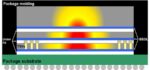
Todd Burkholder and Andras Vass-Varnai, Siemens EDA
As semiconductor devices become smaller, more powerful and more densely integrated, thermal management has shifted from an afterthought to a central challenge in modern IC design. In contemporary 3D IC architectures—where multiple chiplets are stacked and closely arrayed—power… Read More
By now everyone knows that AI has become the all-consuming driver in tech and that NVIDIA GPU-based platforms are the dominant enabler of this revolution. Datacenters worldwide are stuffed with such GPUs, serving AI workloads from automatically drafting emails and summarizing meetings to auto-creating software and controlling… Read More
Designing semiconductor chips has traditionally been costly and controlled by a few major Electronic Design Automation (EDA) vendors—Cadence, Synopsys, and Siemens EDA who dominate with proprietary tools protected by NDAs and restrictive licenses. Fabrication also requires expensive, often export-controlled equipment.… Read More
Silvaco Group, Inc., a veteran player in the EDA and the TCAD space, continues to evolve amid the booming semiconductor industry. Founded in 1984 and headquartered in Santa Clara, California, Silvaco specializes in software for semiconductor process and device simulation, analog custom design, and semiconductor intellectual… Read More
As modern computing systems evolve toward greater parallelism, multithreaded and distributed architectures have become the norm. While this shift promises increased performance and scalability, it also introduces a fundamental challenge: debugging concurrent code. The elusive nature of race conditions, deadlocks, … Read More
GenAI is certainly changing the world. Every day there are new innovations in the use of highly trained models to do things that seemed impossible just a short while ago. As GenAI models take on more tasks that used to be the work of humans, there is always a nagging concern about accuracy and bias. Was the data used to train the model … Read More


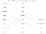


Consolidation and Competition: Who is Winning the $4.5 Billion Interface IP Race?