You are currently viewing SemiWiki as a guest which gives you limited access to the site. To view blog comments and experience other SemiWiki features you must be a registered member. Registration is fast, simple, and absolutely free so please,
join our community today!
WP_Term Object
(
    [term_id] => 157
    [name] => EDA
    [slug] => eda
    [term_group] => 0
    [term_taxonomy_id] => 157
    [taxonomy] => category
    [description] => Electronic Design Automation
    [parent] => 0
    [count] => 4442
    [filter] => raw
    [cat_ID] => 157
    [category_count] => 4442
    [category_description] => Electronic Design Automation
    [cat_name] => EDA
    [category_nicename] => eda
    [category_parent] => 0
    [is_post] =>
)
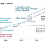
I’ll never forgot working at Intel on a team designing a graphics chip when we wanted to simulate to ensure proper functionality before tapeout, however because of the long run times it was decided to make a compromise to speed things up by reducing the size of the display window to just 32×32 pixels. Well, when first silicon… Read More
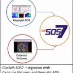
A couple weeks ago I gave a heads-up about a webinar that was being hosted by ClioSoft, Qorvo and Keysight. The topic of the webinar was how to manage custom RF designs across multiple design teams and CAD flows. The webinar was held on February 1st and included presentations by Marcus Ray of Qorvo and Michele Azarian of Keysight.
Much… Read More
Solido Design Automation is rapidly making a name for itself in EDA. Amit Gupta is founder and CEO of Solido Design Automation, based in Saskatoon, Canada. You should also know that Solido is one of the founding members of SemiWiki.com. In the last six years we have published 44 Solido related blogs that have racked up more than 200,000… Read More
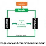
DVCon is fast approaching, less than 3 weeks away. As a verification geek, this must be one of my favorite conferences, so I’ll be there; you’ll see me at tutorials, presentations and wandering around the Exhibit hall. (Pictures here from the 2016 DVCon – many of the same attendees will be at this year’s conference after all :cool:)… Read More
Cadence recently hosted a summit on embedded neural nets, the second in a series for them. This isn’t a Cadence pitch but it is noteworthy that Cadence is leading a discussion on a topic which is arguably the hottest in tech today, with this range and expertise of speakers (Stanford, Berkeley, ex-Baidu, Deepscale, Cadence… Read More
FPGA Design Gets Realby Tom Simon on 02-08-2017 at 12:00 pmCategories: EDA, FPGA, Synopsys
FPGA’s have become an important part of system design. It’s a far cry from how FPGA’s started out – as glue logic between discrete logic devices in the early days of electronic design. Modern day FPGA’s are practically SOC’s in their own right. Frequently they come with embedded processor cores, sophisticated IO cells, DSP,… Read More
When talking to suppliers about their products, conversation tends to focus heavily on what they already have and why it is the answer to every imaginable need in their space. So it’s refreshing when a vendor wants to talk about where customers want to go without claiming they already have the answer wrapped up in a bow. I recently … Read More
Fascinated by computers at a very young age, Peter got his degree in Computer Science and was brought to the Bay Area via AIESEC Berkeley’s student exchange program to write his thesis. He has now more than 15 years of professional experience in software engineering, large scale systems architecture and data center engineering… Read More
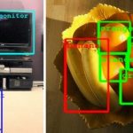
AI and machine learning are two popular buzz words in the high-tech daily news, so you should be getting used to hearing about them by now. What I hadn’t realized was that EDA companies are starting to use machine learning techniques, and specifically targeted at the daunting and compute intensive task of creating SPICE models… Read More
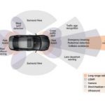
Once upon a time the role of electricity in a car was pretty modest: spark plugs, alternator, lighting, some simple instrumentation and maybe heating, all supported by an equally simple wiring harness (my wife has a 1962 Morris Minor, so I know exactly what the whole wiring harness looks like). How times have changed. Now most or … Read More


Musk’s Orbital Compute Vision: TERAFAB and the End of the Terrestrial Data Center