You are currently viewing SemiWiki as a guest which gives you limited access to the site. To view blog comments and experience other SemiWiki features you must be a registered member. Registration is fast, simple, and absolutely free so please,
join our community today!
WP_Term Object
(
    [term_id] => 157
    [name] => EDA
    [slug] => eda
    [term_group] => 0
    [term_taxonomy_id] => 157
    [taxonomy] => category
    [description] => Electronic Design Automation
    [parent] => 0
    [count] => 4440
    [filter] => raw
    [cat_ID] => 157
    [category_count] => 4440
    [category_description] => Electronic Design Automation
    [cat_name] => EDA
    [category_nicename] => eda
    [category_parent] => 0
    [is_post] =>
)
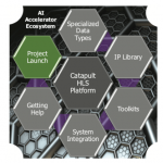
AI accelerators as engines for object or speech recognition (among many possibilities), are becoming increasingly popular for inference in mobile and power-constrained applications. Today much of this inferencing runs largely in software on CPUs or GPUs thanks to the sheer size of the smartphone market, but that will shift… Read More
I will be at SEMICON / EE Design West on Tuesday, July 9, 2019, and so should you!
Quantum computing will be a hot topic at SEMICON West and on Tuesday, July 9, the IBM Quantum Computer will be on display at the Smart Design Pavilion in the South Hall (Moscone Center) from 10:00am to 5:00pm. It looks like no other computer I have ever… Read More
I’m a believer that connectivity for the IoT at scale (the trillions of devices that the industry predicts) has to be cellular. This is partly based on reach, particularly outside urban areas, but is mostly based on the financial implications of that scale. Yes, you can build infrastructure for say local Wi-Fi support with backhaul… Read More
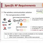
Radio frequency bandwidth has become a precious commodity, with communications companies paying top dollar for prized pieces of the spectrum. However, many radio bands are not often used efficiently. Many existing radio protocols exchange data on a fixed pair of frequencies, tying up those frequencies for other users. When… Read More
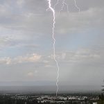
The electrostatic discharge that occurs in lightening, as seen in the picture below, can cause serious damage to the objects on the ground. Over centuries mankind has devised ways, such as lighting rods and arresters, to deflect the energy so it is dissipated harmlessly. The same drama plays out on modern semiconductors due to … Read More
It was inevitable that EDA applications would meet the cloud. EDA has a long history of creating some of the most daunting compute challenges. This arises from employing current generation chips to design the next generation chips. Despite growing design complexity, many tools have kept pace and even reduced runtimes from generation… Read More
SiP is the new SoC @ 56thDACby Tom Dillinger on 06-19-2019 at 6:48 pmCategories: Cadence, EDA, Events
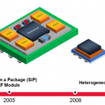
The emergence of 3D packaging technology has been accompanied by the term “more than Moore”, to reflect the increase in areal circuit density at a rate that exceeds the traditional IC scaling pace associated with Moore’s Law. At the recent Design Automation Conference in Las Vegas, numerous exhibits on the vendor floor presented… Read More
Four experts in the discipline of functional safety were gathered together at #56DAC in Vegas earlier in June, hosted at the Mentor booth, so I rested my legs and typed notes as fast as I could. The product areas that I first think about when functional safety (FuSa) comes up are automotive, medical and aerospace, because keeping… Read More
Synopsys seems to particularly excel at these events, whether in half-day tutorials at conferences or, as in this case, in a full-day on-site workshop. You might think there’s not much that can be added in this domain, other than to bring low-power newbies up to speed, but you’d be wrong. This event set the stage with surveys on needs… Read More
Executives from the major EDA companies attend the Design Automation Conference to introduce new product features, describe new initiatives and collaborations, meet with customers, and participate in lively conference panel discussions. Daniel Nenni and I were fortunate to be able to meet with Joe Sawicki, Executive Vice… Read More


Silicon Insurance: Why eFPGA is Cheaper Than a Respin — and Why It Matters in the Intel 18A Era