
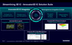
In a major announcement at the 2025 Design Automation Conference (DAC), Siemens EDA introduced a significant expansion to its electronic design automation (EDA) portfolio, aimed at transforming how engineers design, validate, and manage the complexity of next-generation three-dimensional integrated circuits (3D ICs).… Read More
Siemens EDA Unveils Groundbreaking Tools to Simplify 3D IC Design and Analysis


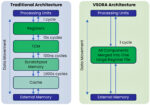
TSMC CoWoS versus Intel EMIB Semiconductor Packaging