Increasingly complex heterogeneous packaging solutions have proved essential to meeting the rapidly scaling requirements for automotive electronics. Perhaps there is no better example of this than advanced driver-assistance systems (ADAS) that are found in most new cars. In a recent paper published by Siemens EDA, they detail the current technology trends that are creating design challenges. The paper titled “Methodology and Process for Heterogeneous Automotive Package Design” mentions shrinking bump pitch, increasing bump density, decreasing ball pitch, high current consumption and high frequency issues as factors that must be addressed to meet system level requirements in this market.
The Siemens paper is focused on the adoption of Xpedition Substrate Integrator (xSI) from Siemens by the Back-End Manufacturing Technology Team at ST Microelectronics in Agrate Italy. The design of their current and future ADAS products requires a tool that can handle increasing package connectivity density and deal with design data from chip and PCB tools as well as the package design. The paper outlines a well-structured three phase flow for package design.
In the early stage there is focus on design rule identification, implementation technology, cost optimization, and design strategy verification. All aspects of the design are explored to come up with a preliminary implementation. The areas considered are package dimensions, substrate stack up, ball-out definitions, break out strategies and preliminary connectivity assignment. With this information, cost and performance metrics can be estimated.
This is followed by the intermediate stage, where attention is paid to physical design, debugging and optimization. A lot happens here, starting with finalization and optimization of the substrate routing. Key aspects such as manufacturability, interfaces, power requirements and more are assessed. The final stage involves verification and sign off of every aspect of the finished design. This includes thermal, signal integrity, power integrity and manufacturing verification leading to the tape-out handoff to manufacturing.
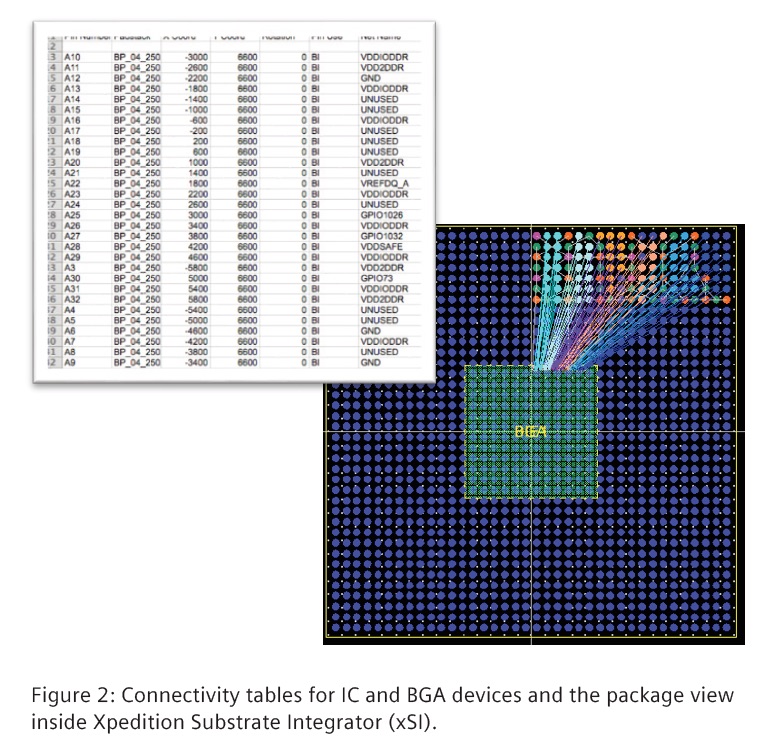
The Siemens paper points out that each of these design stages rely heavily on co-design, co-simulation and co-optimization. Without these a siloed non-convergent design process would result. It is necessary for the package design flow to take a system level approach. This is the only way that system connectivity can be optimized to meet all requirements. Data must flow from IC and PCB tools. xSI helps eliminate the use of spreadsheets for passing preliminary data by providing a feature known as connectivity tables to capture system definition during development. This has the added benefit of permitting easy what-if analysis.

Siemens xSI was attractive to ST because of its extensive support for early prototyping during the package design process. Missing devices can be created from scratch, and complex bump and ball pitch and positions can be defined for sophisticated design exploration. Because the design is not static, xSI supports fast connectivity updates when design elements are changed via ECO. The article describes several other innovative capabilities that influenced ST’s decision.
The article also describes in some detail the test case that was used by ST. At the end of the article the authors review the most important aspects of the flow that xSI offers. They point out that xSI enables hierarchical construction of the complete package assembly with step-by-step handling of multiple parts, including reuse of parts. In order to meet the needs of high-speed interface design and accommodate complex bump-out geometries, xSI includes efficient integration with external tools, and flexibility during IC-package connectivity planning and optimization.
Package design is by its very nature heavily constrained. Both physically, by its role in between die and board, but also because of interface and interconnection requirements. There are thermal, power, signal integrity, area and many other requirements to satisfy. There is also no argument that ADAS systems impose some of the strictest requirements on system operation. They often include high speed video streams, display output, as well as other sensor input and control output. ADAS systems also include extremely advanced conventional and AI processors. Siemens offers a lot of information about why ST chose xSI in the article, which is available here on the Siemens website.
Also Read:
Electromigration and IR Drop Analysis has a New Entrant
Formal Methods for Aircraft Standards Compliance
Verifications Horizons 2021, Now More Siemens
Share this post via:


Comments
There are no comments yet.
You must register or log in to view/post comments.