
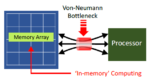
“AI is the new electricity.”, according to Andrew Ng, Professor at Stanford University. The potential applications for machine learning classification are vast. Yet, current ML inference techniques are limited by the high power dissipation associated with traditional architectures. The figure below highlights the … Read More

Author: Tom Dillinger
In-Memory Computing for Low-Power Neural Network Inference
A Compelling Application for AI in Semiconductor Manufacturing

There have been a multitude of announcements recently relative to the incorporation of machine learning (ML) methods into EDA tool algorithms, mostly in the physical implementation flows. For example, deterministic ML-based decision algorithms applied to cell placement and signal interconnect routing promise to expedite… Read More
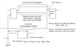
Contact over Active Gate Process Requirements for 5G

Summary
A recent process enhancement in advanced nodes is to support the fabrication of contacts directly on the active gate area of a device. At the recent VLSI 2020 Symposium, the critical advantages of this capability were highlighted, specifically in the context of the behavior of RF CMOS devices needed for 5G designs.
Introduction… Read More
Optimizing Chiplet-to-Chiplet Communications
Summary
The growing significance of ultra-short reach (USR) interfaces on 2.5D packaging technology has led to a variety of electrical definitions and circuit implementations. TSMC recently presented the approach adopted by their IP development team, for a parallel-bus, clock-forwarded USR interface to optimize power/performance/area… Read More
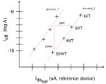
Multi-Vt Device Offerings for Advanced Process Nodes
Summary
As a result of extensive focus on the development of workfunction metal (WFM) deposition, lithography, and removal, both FinFET and gate-all-around (GAA) devices will offer a wide range of Vt levels for advanced process nodes below 7nm.
Introduction
Cell library and IP designers rely on the availability of nFET and pFET… Read More
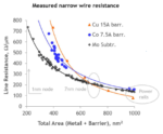
Design Technology Co-Optimization (DTCO) for sub-5nm Process Nodes
Summary
Design Technology Co-Optimization (DTCO) analysis was pursued for library cell PPA estimates for gate-all-around (GAA) devices and new metallurgy options. The cell design and process recommendations are a bit surprising.
Introduction
During the “golden years” of silicon technology evolution that applied Dennard… Read More
Embedded MRAM for High-Performance Applications
Summary
A novel spin-transfer torque magnetoresistive memory (STT-MRAM) IP offering provides an attractive alternative for demanding high-performance embedded applications.
Introduction
There is a strong need for embedded non-volatile memory IP across a wide range of applications, as depicted in the figure below.
The… Read More
Emerging Requirements for Electromagnetic Crosstalk Analysis

This article will describe the motivations for pursuing a new flow in the SoC design methodology. This flow involves the extraction, evaluation, and analysis of a full electromagnetic coupling model for a complex SoC and its package environment. The results of this analysis highlight the impact of electromagnetic coupling… Read More
Ultra-Short Reach PHY IP Optimized for Advanced Packaging Technology

Frequent Semiwiki readers are no doubt familiar with the rapid advances in 2.5D heterogeneous multi-die packaging technology. A relatively well-established product sector utilizing this technology is the 2.5D integration of logic die with a high-bandwidth memory (HBM) DRAM die stack on a silicon interposer; the interposer… Read More
Useful Skew in Production Flows
The concept of applying useful clock skew to the design of synchronous systems is not new. To date, the application of this design technique has been somewhat limited, as the related methodologies have been rather ad hoc, to be discussed shortly. More recently, the ability to leverage useful skew has seen a major improvement,… Read More


Musk’s Orbital Compute Vision: TERAFAB and the End of the Terrestrial Data Center