At DAC in 2012 I visited a few dozen EDA companies and blogged 32 articles, however I didn’t get to see what Apache Design (now a subsidiary of ANSYS) had to say. I did have 20 minutes today to watch their latest video on SoC Power Integrity Challenges and decided to share what I learned. If you want to watch the video at Tech Online,… Read More
Author: Daniel Payne
IC Test Debug at Altera
My background is IC design engineering, so it’s always a delight to talk with another engineer on their chip challenges. Today I spoke by phone with Sucharita Biswas, a Senior Hardware Engineer at Altera involved in IC test debug for FPGA devices.
RTL Restructuring
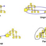
Hierarchical IC design has been around since the dawn of electronics, and every SoC design today will use hierarchy for both the physical and logical descriptions. During the physical implementation of an SoC you will likely run into EDA tool limits that require a re-structure of the hierarchy. This re-partitioning will cause… Read More
Circuit Analysis & Debugging
In EDA we often talk about how fast a SPICE circuit simulator is, or about capacity and accuracy compared to silicon measurements. Yes, speed, capacity and accuracy are important, however when talking to actual transistor-level circuit designers you discover something quite different, most of their time is spent doing debugging,… Read More
An Analog IC Router
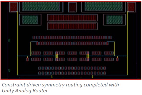
Earlier this week I wrote about a Goliath in EDA, Synopsys, and their new analog router, today it’s the David in EDA, Pulsic and their Unity Analog Router. I spoke with several people from Pulsic by phone:
- Christopher Jost – San Jose
- Dave Noble – San Jose
- Fumiaki Sato – Tokyo, Japan
A New Mixed-Signal IC Router
Pure digital routers for IC designs have an easier task than mixed-signal routers, because mixed-signal routers have more constraints like:
- Shielded buses
- Differential pairs
- Twisted pairs
- Matched RC routing
- 20nm technology rules
- Double Patterning Technology (DPT)
Unlocking the Full Potential of Soft IP
EDA vendors, IP suppliers and Foundries provide an eco-system for SoC designers to use in getting their new electronic products to market quicker and at a lower cost. An example of this eco-system are three companies (TSMC, Atrenta, Sonics) that teamed up to produce a webinar earlier in March called: Unlocking the Full Potential… Read More
View from the top: Brad Quinton
Many engineers dream about starting their own company some day, and today I talked with an engineer that has gone beyond the dreaming stage to actually start an EDA company and then get that company acquired. His name is Brad Quinton and the start-up was called Veridae Systems, now part of Tektronix.
Brad Quinton… Read More
Interconnect Optimization of an SoC Architecture
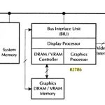
My last chip design at Intel was a GPU called the 82786and the architects of the chip wrote a virtual prototype using the MAINSAIL language. By using a virtual prototype they were able to:
- Simulate bus traffic, video display and video RAM
- Determine throughput
- Measure latency
- Verify that bus priorities were working
- Optimize the
Visual Debugging at Altera on Billion-Transistor Chips
My first job out of college was doing transistor-level circuit design, so I’m always curious about how companies are doing billion-transistor chip design and debug these days at the FPGA companies.
I spoke with Yaron Kretchmer,he works at Altera and manages the engineering infrastructure group where they have a compute… Read More










Solving the EDA tool fragmentation crisis