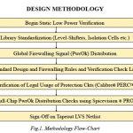
IC designer Shubhyant Chaturvediof AMD used EDA tools from Mentor Graphicsand Concept Engineeringto perform static, low-power verification of a mixed-signal SoC design with a combined CPU and GPU. Shubhyant presented a poster session at DAC two weeks ago in Austin, and I wanted to share it with my readers here at SemiWiki.… Read More
Author: Daniel Payne
IC Variability Analysis at DAC
There were a handful of EDA vendors at DAC this year touting tools for IC variability analysis. On Tuesday I met with Firas Mohamed, CEO and President of Infiniscale.… Read More
A New STA Tool at DAC, No Not Cadence
The big EDA companies get big attention at DAC, however sometimes the little EDA start-ups like Arcadia Innovationhave a new product that can be overlooked. On Tuesday at DAC I met with Joey Lin, founder of Arcadia Innovation and learned about his new STA (Static Timing Analysis) tool called TimeHawk .… Read More
Physical IP Update at DAC
Last year at DAC I visited this little-known physical IP company called DXCorr, so I decided to visit them again this year and get an update.… Read More
Deploying 14nm FinFETs in your Next Mobile SoC
At DAC in Austin a design company, foundry and EDA vendor teamed up to present their experiences with 14nm FinFETs during a breakfast on Tuesday.
Panelists included:
- Ed Sperling, Semi Mfg and Design
- Anil Jain, Cavium
- Subramani Kengeri, GLOBALFOUNDRIES
- Kelvin Low, GLOBALFOUNDRIES
- Raymond Leung, Synopsys
- Bari Biswas, Synopsys
Eldo and Pyxis from Mentor, DAC Update
Last Monday at DAC I met with Linda Fosler, Marketing Director at Mentor Graphics to get an update on what’s new with Eldo(Circuit simulator) and Pyxis (custom IC layout and schematic).
Linda Fosler, Mentor Graphics… Read More
Calibre Update at DAC
Mentor Graphics throws a very nice dinner party at DAC each year for journalists, bloggers and top customers, so this year I spoke with Michael Buehler-Garcia about what’s new with Calibre.
Michael Buehler-Garcia, Mentor Graphics
… Read More
Tela Innovations, DAC Update
Lawsuits in EDA are common, and Tela Innovationsfiled a huge complaint back in February with the U.S. International Trade Commission (USITC) against HTC Corporation; HTC America, Inc.; LG Electronics, Inc.; LG Electronics U.S.A., Inc.; LG Electronics MobileComm U.S.A., Inc.; Motorola Mobility LLC; Nokia Corporation; Nokia,… Read More
GPU-Based SPICE Simulator for Library Characterization
Jeff Tuanis the CEO and President of an EDA startup called G-Analog, founded in May 2012. His background includes working at: Cadence, Epic, Synopsys, Nassda, Chartered Semi and GLOBALFOUNDRIES. Jason Lu is the R&D manager. We met at DAC last week to talk about his company’s new product called Gchar for IC library characterization… Read More
Custom Physical IC Design update from Cadence
Custom IC design and layout is becoming more difficult at 20nm and smaller nodes, so the EDA tools have to get smarter and work harder for us in order to maintain productivity with the fewest iterations to reach our specs. Dave Stylesand John Stabenow of Cadence met with me last Monday in Austin at the DAC exhibit area.
John Stabenow… Read More


Intel, Musk, and the Tweet That Launched a 1000 Ships on a Becalmed Sea