You are currently viewing SemiWiki as a guest which gives you limited access to the site. To view blog comments and experience other SemiWiki features you must be a registered member. Registration is fast, simple, and absolutely free so please,
join our community today!
Power transistors are commonly used in applications like: hybrid vehicles, electric vehicles, automotive, home appliances, LED lighting, TVs, power and energy. In the old days an engineering team could build their device with power transistors, then after production run some thermal testing to see if they guessed the proper… Read More
The first consumer products with 20nm processing are arriving in 2014 like the 2 billion transistor A8 chip in the iPhone 6, however at the 14nm node there are new designs underway to continue the trend of Moore’s Law. To get a better feel for the challenges of designing with 14nm FinFET technology I watched a 23 minute video … Read More
FPGA devices are a great way to drive silicon technology development because they contain both digital and analog IP, along with sophisticated IO cells. The highest performance IOs are transceivers, and Altera has recently designed the Arria 10 device family to include up to 96 transceivers, using a 20nm technology that can achieve… Read More
In America the popular press talks almost non-stop about: Disasters, politicians, celebrities and Apple. Yes, Apple. Today I watched the live cast of the new Apple product announcements.
iPhone 6
First, the see things differently video started playing, then the live stream died so I had to turn over to CNET where they were live … Read More
The server market is a diverse, yet standardized market. The ICs and components designed and manufactured in final assemblies must meet form factor requirements for rack mount and blades. The form factor enclosures and the component placement dictate the thermal-mechanical properties and hence the thermal cooling limits … Read More
The periodic table shows that Silicon (Si) is in a column along with other elements like Carbon (C) and Germanium (Ge). With so much emphasis on Silicon, you’d think that the other semiconductor materials have been neglected a bit.
Silicon is a wonderful material and most of our consumer electronics and handheld devices … Read More
In college many of us dreamed of starting up our own company by offering something new that has never been done before. Today I spoke by phone with Yunshan Zhuin Shanghai, and he has actually lived out this scenario by founding NextOp in 2006, then getting that company acquired by Atrentain 2012. The new capability that NextOp created… Read More
IC designers have been running analysis tools for power, noise and reliability for many years now, so what is new when you start using FinFET transistors instead of planar transistors? Calvin Chow from ANSYS (Apache Design) presented on this topic earlier in the summer through a 33 minutewebinar that has been archived. There is… Read More
RTL designers know that their code gets transformed into gates and cells by using a logic synthesis tool, however these gates and cells are further comprised of transistors and sometimes you really need to optimize the transistor sizing to reach power, performance and area goals. I’ve done transistor-level IC design before,… Read More
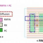
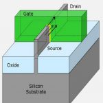
Planar CMOS processes have been offered for decades now, and all the way down through the 28nm node it has been riding the benefits of Moore’s Law. A few years back we started hearing from Intel about TriGate (aka FinFET) starting at the 22nm node as a way to use a more 3D processing approach for transistors instead of planar CMOS.… Read More


Why Your LLM-Generated Testbench Compiles But Doesn’t Verify: The Verification Gap Problem