You are currently viewing SemiWiki as a guest which gives you limited access to the site. To view blog comments and experience other SemiWiki features you must be a registered member. Registration is fast, simple, and absolutely free so please,
join our community today!
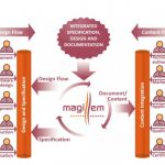
One challenge in SoC projects is maintaining consistency between the specification, design and documentation throughout the product lifecycle. Imagine the chaos if your specification for power is 300 mW, the design is actually 350 mW and the documentation promises 250 mW. Traditionally the design and documentation process… Read More
My old headphones with microphone lost a channel, so it was time to upgrade and I went shopping for something that had high fidelity and fit over my ears, instead of on my ears. After some online research I opted for the Bose headphones, because that brand has been around for decades, they offer many models to choose from, and are readily… Read More
When I hear the phrase Static Timing Analysis (STA) the first EDA tool that comes to mind is PrimeTimefrom Synopsys, and this type of tool is essential to reaching timing closure for digital designs by identifying paths that are limiting chip performance. Sunil Walia, PrimeTime ADV marketing lead spoke with me by phone on Thursday… Read More
When chip designers moved from a gate-level design methodology to coding with RTL there was a learning curve involved, and the same thing happens when you move from RTL to High Level Synthesis (HLS) using C++ or SystemC coding. One great shortcut to this learning curve is the use of pre-defined library functions. I just heard about… Read More
This month I upgraded my TV at home with a 40″ LED set from Samsung, Denon AV receiver and Samsung Blu-ray player. Also being a Google fan I bought a Chromecast device.
At CES there were multiple announcements from Intel, and one that caught my eye was the Intel Compute Stick because it reminded me of the Google Chromecast device… Read More
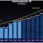
SemiWiki blogger Eric Esteve does an excellent job writing about all of the semiconductor IP available, and the popularity of IP is only growing more each year. Here’s a projection from IBS about semiconductor IP showing revenues of $4.7B by 2020:
Analyst Gary Smith divides IP into three broad categories: Functional, Foundation… Read More
My first experience with logic synthesis was at Silicon Compilers in the late 1980s using a tool called Genesil. Process technology since that time has moved from 3 um down to 20 nm, so there are new challenges for RTL synthesis. Today you can find logic synthesis tools being offered by the big three in EDA: Synopsys, Cadence, Mentor… Read More
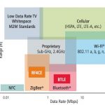
Wireless technology is all around as I use cellular on an Android phone, WiFi to connect my MacBook Pro to the internet, Bluetooth for a headset, ANT+ for my cycling computer, and NFC to speed up electronic payments on the Android phone. Here’s a big picture look at some of the modern wireless standards available to choose from:… Read More
I’m an avid cyclist that rode some 6,744.3 miles in 2014, according to www.strava.com, a free web site and popular app for road bikers like me. At CES this week I’ve read about many creative devices and apps to make your cycling experience better, so here’s my take on all of it.… Read More
Right now I’m typing on my MacBook Pro computer connected to the Internet through WiFi, thanks to the electronics in both my laptop and WiFi router. I kind of take WiFi for granted because it is so ubiquitous throughout my daily life, yet there are IC designers at companies like Lantiq Semiconductorthat have to design and optimize… Read More


Why Your LLM-Generated Testbench Compiles But Doesn’t Verify: The Verification Gap Problem