You are currently viewing SemiWiki as a guest which gives you limited access to the site. To view blog comments and experience other SemiWiki features you must be a registered member. Registration is fast, simple, and absolutely free so please,
join our community today!
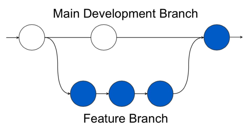
Linux creator Linus Torvalds lives in Oregon not too far from me and he also created the popular Git system for Design Management (DM) in 2004 that is now used by many software developers. So what makes Git so attractive as a DM tool?
- Feature-branch workflow
- Easy to switch context between features
- New features can be created orderly
…
Read More
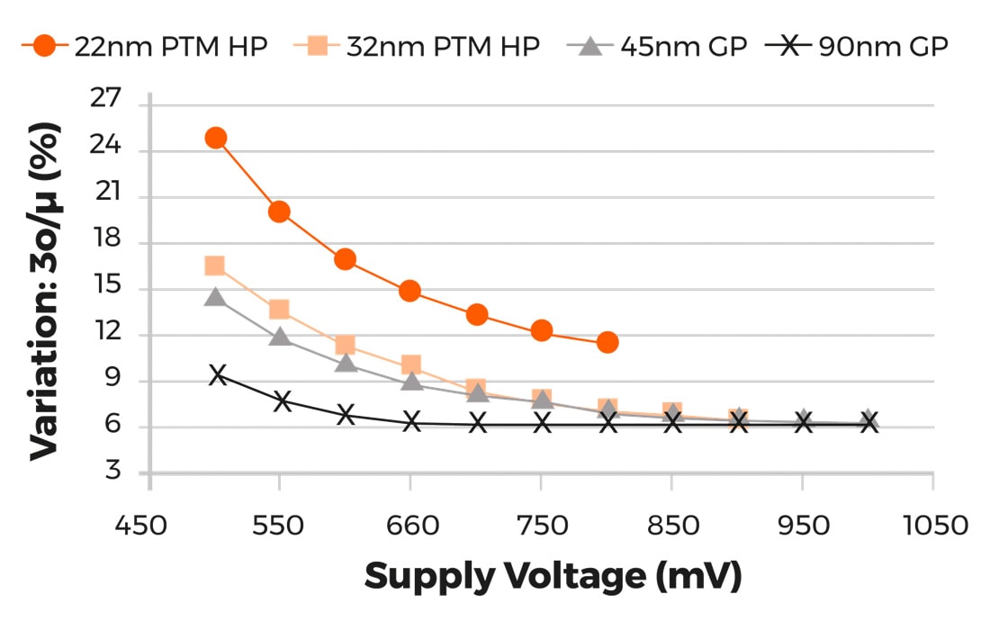
At Intel back in the late 1970’s we wanted to know what process corner each DRAM chip and wafer was trending at so we included a handful of test transistors in the scribe lines between the active die. Having test transistors meant that we could do a quick electrical test at wafer probe time to measure the P and N channel transistor… Read More
I’ve been driving cars since 1975 and in the early days we had simplistic gauges for feedback like: Speed, Fuel level, Oil level, RPM. Back then when you popped the hood of a car you could see through the engine compartment onto the ground below, however with today’s cars the engine compartments are crammed with tubes,… Read More
I come from a car-centric family where my father actually bought and sold over 300 vehicles in his lifetime, so automotive mega-trends pique my interest. A new conference called Semiconductors ISO 26262 held it’s first annual event last month, meeting in Munich with guest speakers from some impressive companies like: … Read More
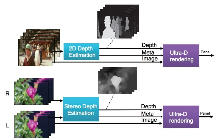
In the blur of activities at DAC last year I visited the Mentor booth a few times and had just a few minutes to glance at a 3D TV display that didn’t require me to wear any funny glasses, kind of novel I thought at the time because I’ve read that the market of 3D TV sets is being hampered by requiring viewers to wear glasses. The… Read More
2017 was a banner year for semiconductor sales as they topped $400B for the first time, an increase of some 20%, there is happiness in Silicon Valley, Taiwan, South Korea, and well, everywhere. With the foundries pushing to ever-smaller process dimensions and even going back to mature nodes and offering more variations that are… Read More
I’m an avid road bike enthusiast having just completed my 2017 goal of 13,000 miles, so follow me on Strava if you want to see the routes and photo adventures I have in Oregon. In the photo below I’m the guy in the middle with the Portland Velojersey on and we’re in a parking lot just 2 blocks away from Intel’s… Read More
Semiconductor IP re-use is a huge part of the productivity gains in SoC designs, so instead of starting from a clean slate most chip engineers are re-using cells, blocks, modules and even sub-systems from previous designs in order to meet their schedule and stay competitive in the market place. But what happens when you intend to… Read More
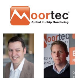
Six years ago I first interviewed Stephen Crosher, CEO and Co-founder of Moortecas they were in startup mode with some new semiconductor IP for temperature sensing, and earlier this month I attended their webinar all about embedded in-chip monitoring to get caught up with their technology and growing success. Ramsay Allen is … Read More
Our smart phone driven semiconductor economy consumes a lot of IP blocks to enable quick product development cycles, often annually updating with new models to choose from. So where do you find all of the best semiconductor IP, verification IP and embedded software? Well, one place is at the 2nd annual REUSE conference, scheduled… Read More


Captain America: Can Elon Musk Save America’s Chip Manufacturing Industry?